Eureka AIR delivers breakthrough ideas for toughest innovation challenges, trusted by R&D personnel around the world.

Method of packing silicon and packing body

Active Publication Date: 2009-03-05
MITSUBISHI MATERIALS CORP
View PDF16 Cites 19 Cited by
  • Summary
  • Abstract
  • Description
  • Claims
  • Application Information

AI Technical Summary

Benefits of technology

[0010]The present invention takes the above circumstances into consideration, with an object of providing a method of packing silicon and a packing body capable of: suppressing vibrations of silicon mainly such as lump of polycrystalline silicon, with a simple method; further reducing generation of fine powder due to rubbing between the silicon and a packing bag; and avoiding a reduction in the quality of the silicon.

Problems solved by technology

However, since this lump of polycrystalline silicon is a brittle material, the edges of the cut surfaces and the edges of the crushed surfaces are often sharp.
However, vibrations still cause rubbing between the lump of polycrystalline silicon and the surface of the packing bag, and the lump of polycrystalline silicon and the packing body become pulverized in some cases.
If fine powder of such polycrystalline silicon lump and polyethylene resin is brought into the above mentioned quartz crucible together with the lump of polycrystalline silicon, it causes crystal defects in the single crystal silicon produced after being pulled out of the quartz crucible, and consequently causes a reduction in the quality of a silicon single crystal.
Therefore, in the case where the methods disclosed in Patent Document 1 and Patent Document 2 are used, since the vibrations received by the polycrystalline silicon lump are not reduced, suppression of fine powder generation is limited.
However, there is a problem in that in order to reduce vibrations further, use of a large amount of polystyrene foam is necessary, and there is a cost for after-use processing and a negative impact on the environment.

Method used


Image

  • Method of packing silicon and packing body
  • Method of packing silicon and packing body
  • Method of packing silicon and packing body

Examples


Embodiment Construction

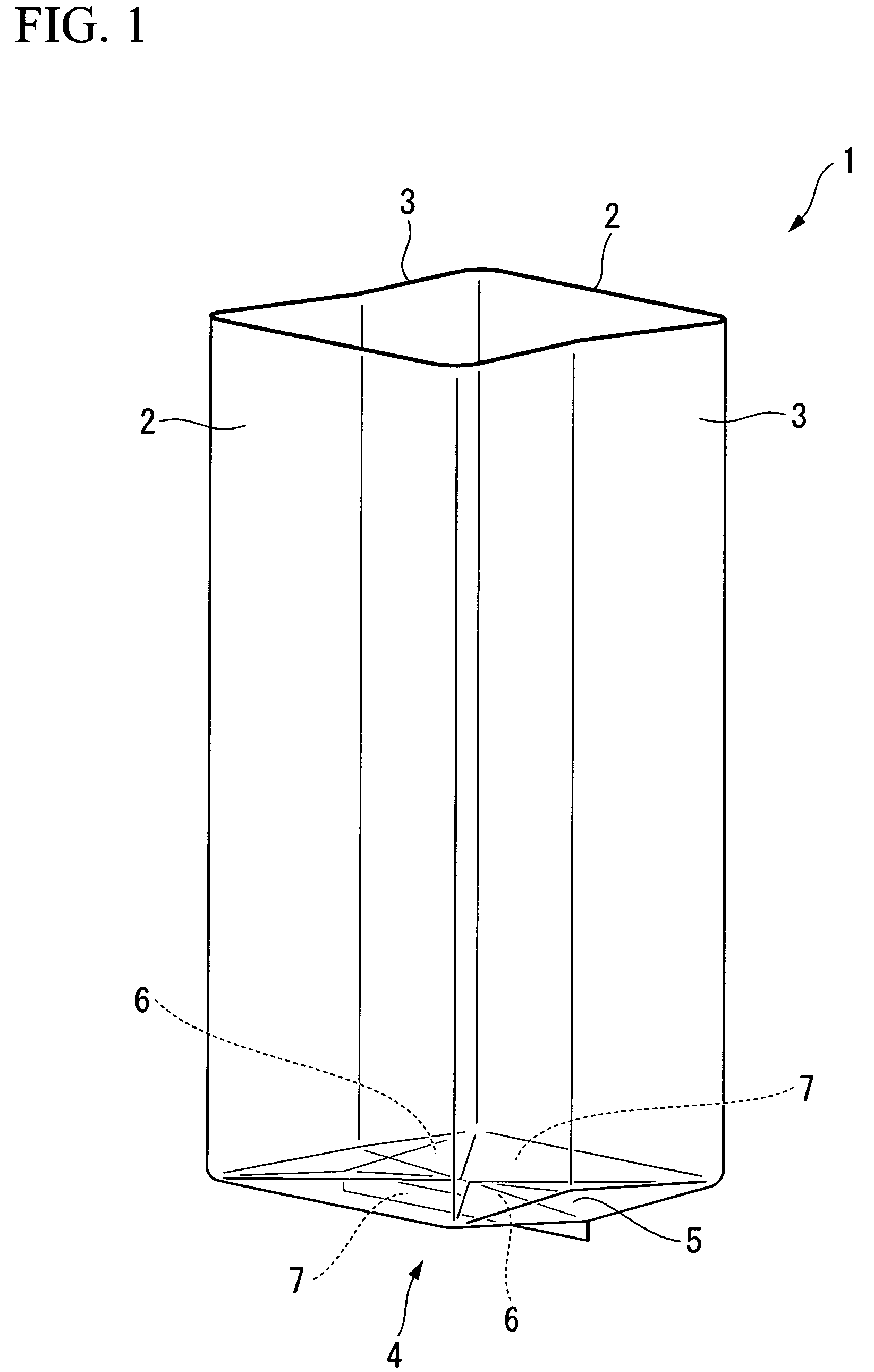
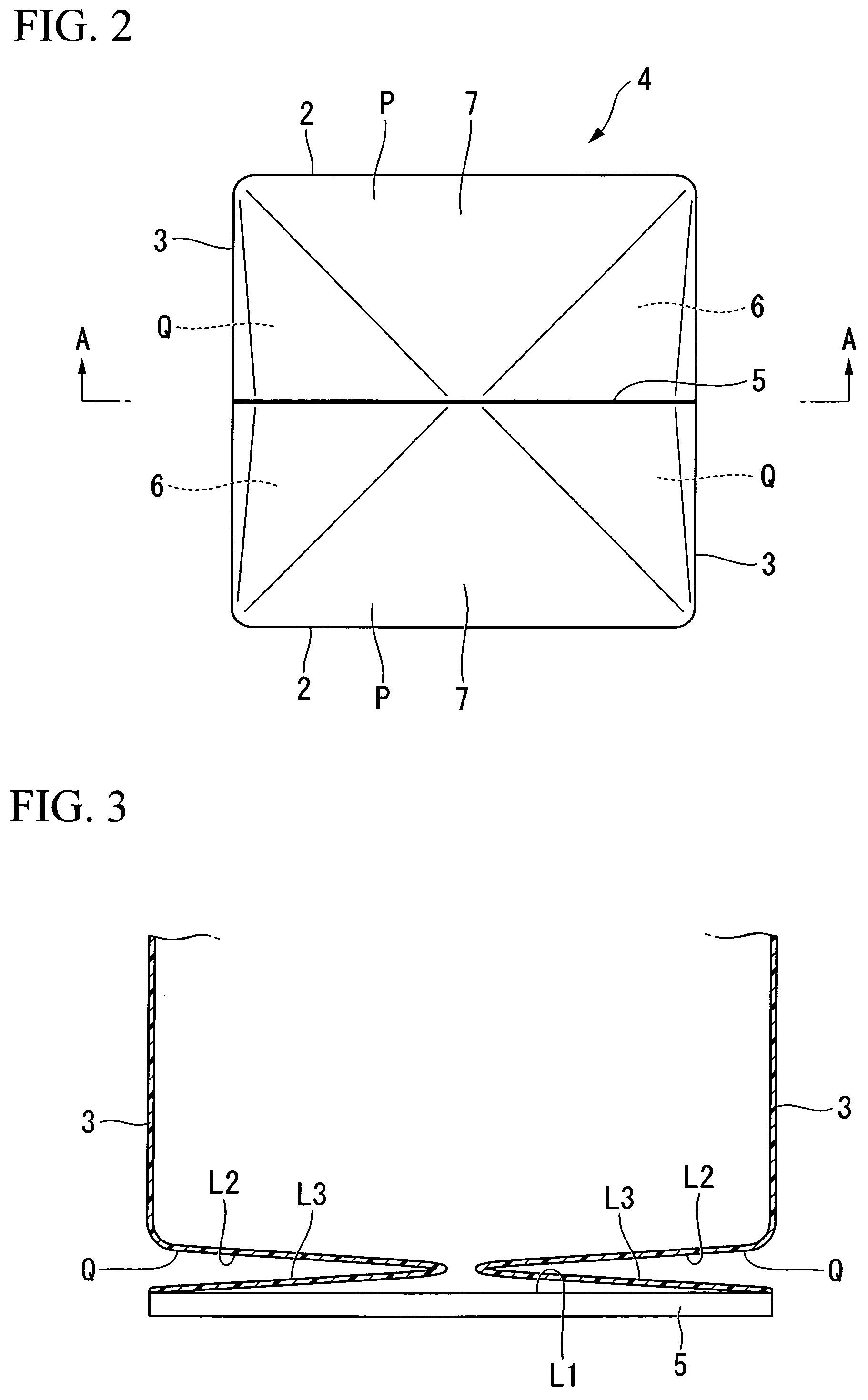
[0032]Hereunder, a method of packing silicon and a packing body according to an embodiment of the present invention is described, with reference to the accompanying drawings. FIG. 1 is a perspective view of a packing bag to be used as an inner bag or an outer bag of the present embodiment. A packing bag 1 is formed for example from a transparent film such as polyethylene resin, and has a cross-sectionally substantially square bottomed bag shape with four side face sections 2 and 3 and a bottom section 4. Among the four side face sections 2 and 3, each of a pair of the opposing side face sections 2 has a substantially planar state. In another pair of the opposing side face sections 3, there are provided inward fold lines, which are for valley-folding, along the longitudinal direction to allow the packing bag 1 to be folded into a small size. The packing bag 1 is folded along these fold lines into a small size when not in use, and is expanded into a bag shape when used.

[0033]In this p...


PUM

PropertyMeasurementUnit
Angleaaaaaaaaaa

Abstract

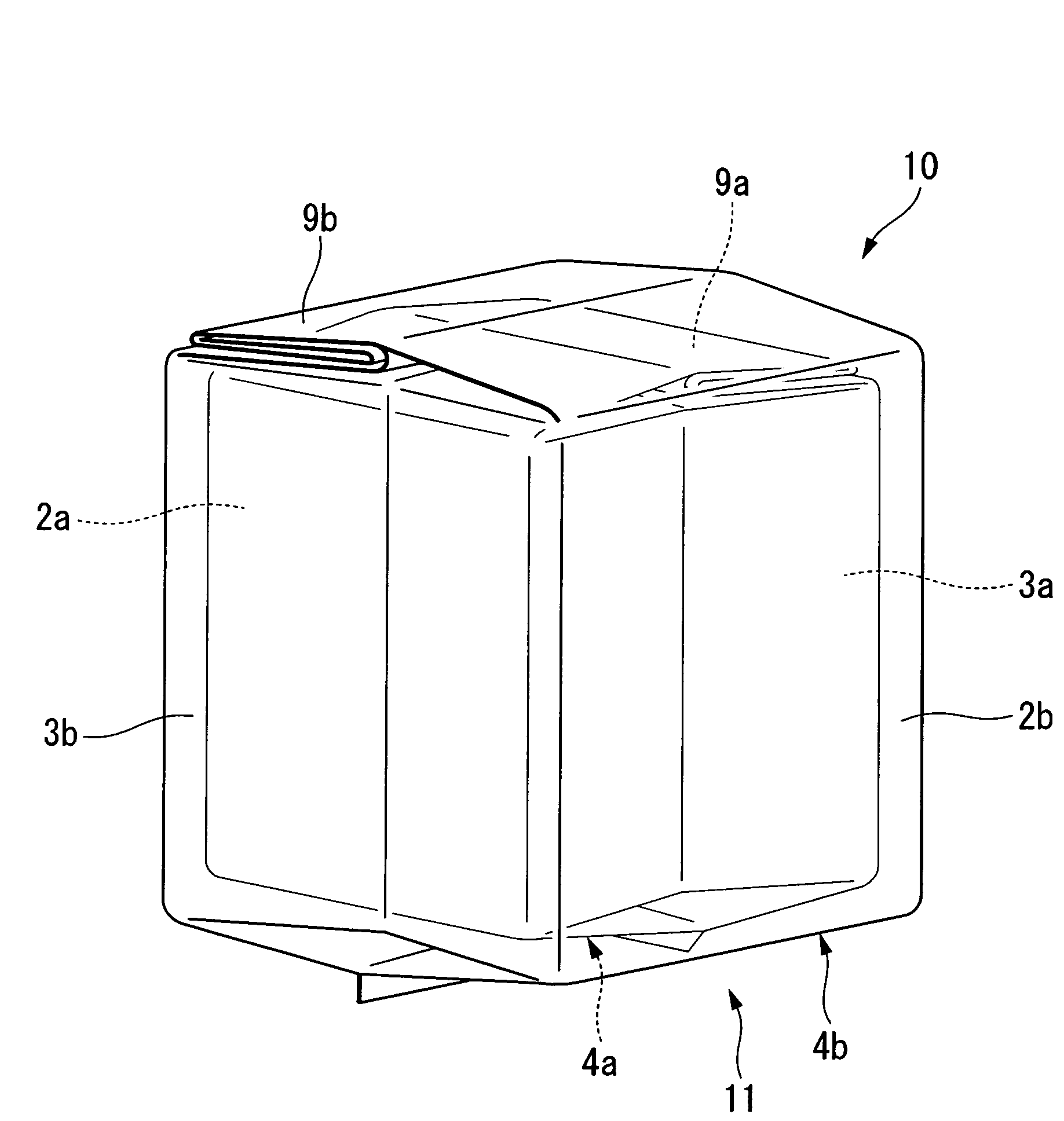
When packing a polycrystalline silicon with a two-layer structured packing body comprising an inner bag (1a) and an outer bag (1b), there are used the inner bag (1a) and the outer bag (1b) having bottom sections (4a, 4b) provided with a pair of tucked sections, the shape of which is substantially a triangle in plan view, formed by inward-folding the portions continued from both of rectangular side face sections (3a, 3b), and when storing the inner bag (1a) that stores the polycrystalline silicon therein into the outer bag (1b), the bottom sections (4a, 4b) are superimposed with the respective tucked sections (6a, 6b) of the inner bag (1a) and the outer bag (1b) displaced from each other by 90° so that they do not overlap on each other.

Description

CROSS-REFERENCE TO RELATED APPLICATION[0001]Priority is claimed on Japanese Patent Application No. 2007-220221, filed Aug. 27, 2007, and Japanese Patent Application No. 2008-179628, filed Jul. 9, 2008, the content of which are incorporated herein by reference.BACKGROUND[0002]1. Technical Field[0003]The present invention relates to a method of packing silicon and a packing body, the primary packing object of which is polycrystalline silicon used as molten material when manufacturing single crystal silicon.[0004]2. Related Art[0005]As a method of manufacturing single crystal silicon, there is known the Czochralski method (hereunder, referred to as the CZ method). This CZ method has an advantage in that a large diameter high-purity silicon single crystal in a dislocation-free state or in a state of having very low lattice defects can be easily obtained.[0006]In the CZ method: high-purity polycrystalline silicon is placed in a quartz crucible and melted in a furnace; the silicon melt is...

Claims


Application Information

Patent Timeline
IPC IPC(8): B65B11/58
CPCB65D31/04B65D81/03B65D31/08B65D31/16B65D71/40
Inventor SASAKI, GO
Owner MITSUBISHI MATERIALS CORP
Why Eureka
Eureka Blog
Learn More