Sputtering method and apparatus

Active Publication Date: 2009-03-05
FUJIFILM CORP
View PDF11 Cites 10 Cited by
  • Summary
  • Abstract
  • Description
  • Claims
  • Application Information

AI Technical Summary

Benefits of technology

[0068]The film deposition method of the present invention is so designed that the conditions of film deposition are determined based on the relation between the above-mentioned two factors that affect the film characteristics and the characteristics of the film deposited; as a result, films of good quality can be deposited consistently by plasma-enhanced vapor-phase growth techniques such as sputtering. Consequently, the film deposition method of the present invention can preferably be applied in depositing thin films such as piezoelectric fi

Problems solved by technology
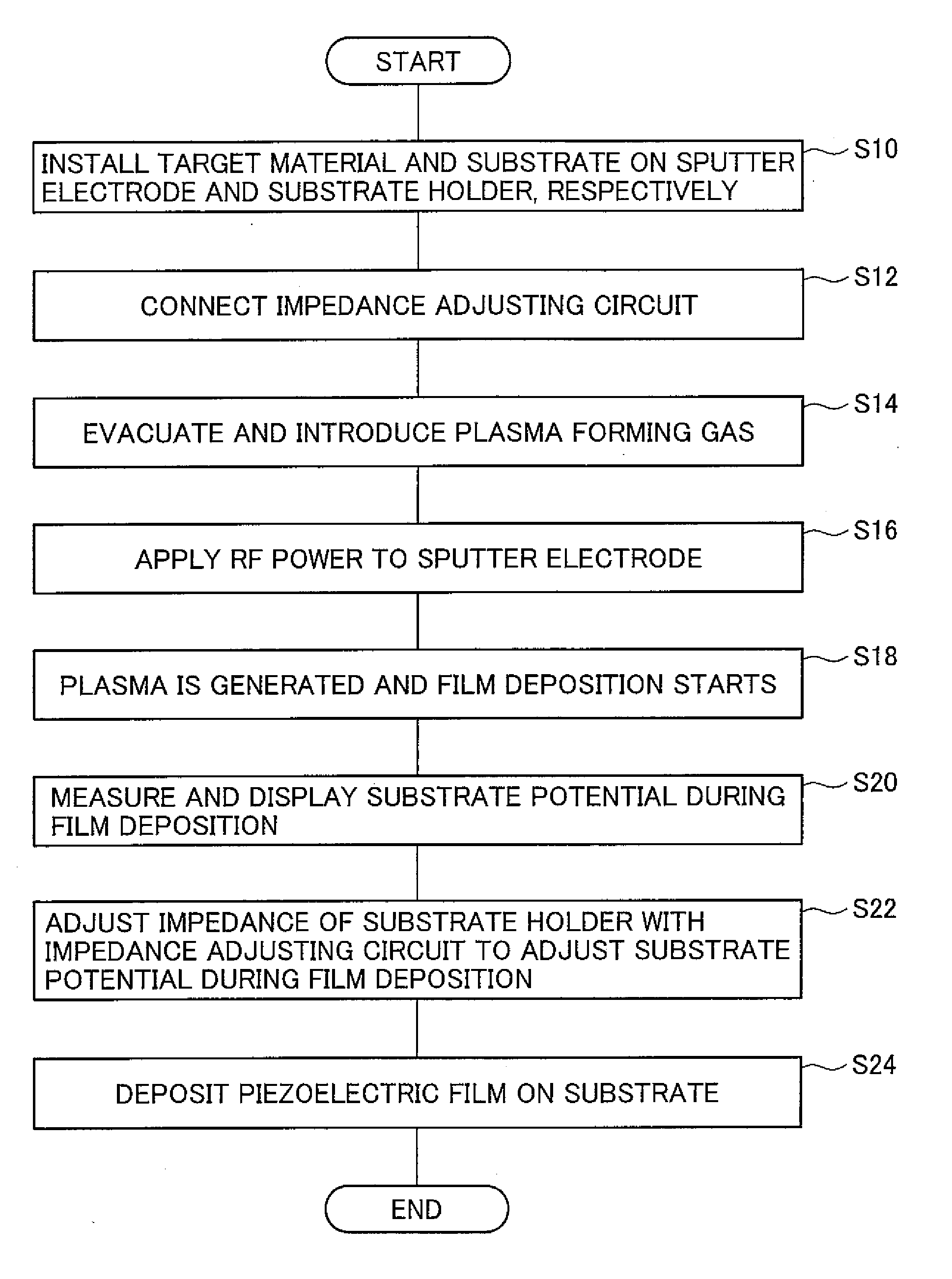
Problems with the bias sputtering method and apparatus that are described in JP 06-145972 A are that in all cases that are proposed, the substrate electrode is connected to a DC or AC power source for applying a predetermined potential to a surface of the substrate and, what is more, the third electrode, or the alternately applying means and the matching circuit control means, or the floating potential detection means or the RF current detection means in combination with the substrate potential control means must be provided, which inevitably adds to the complexity of the apparatus design or the way it is controlled.
There is a further problem with the invention described in JP 06-1

Method used


Image

  • Sputtering method and apparatus
  • Sputtering method and apparatus
  • Sputtering method and apparatus

Examples


Example

Example 1

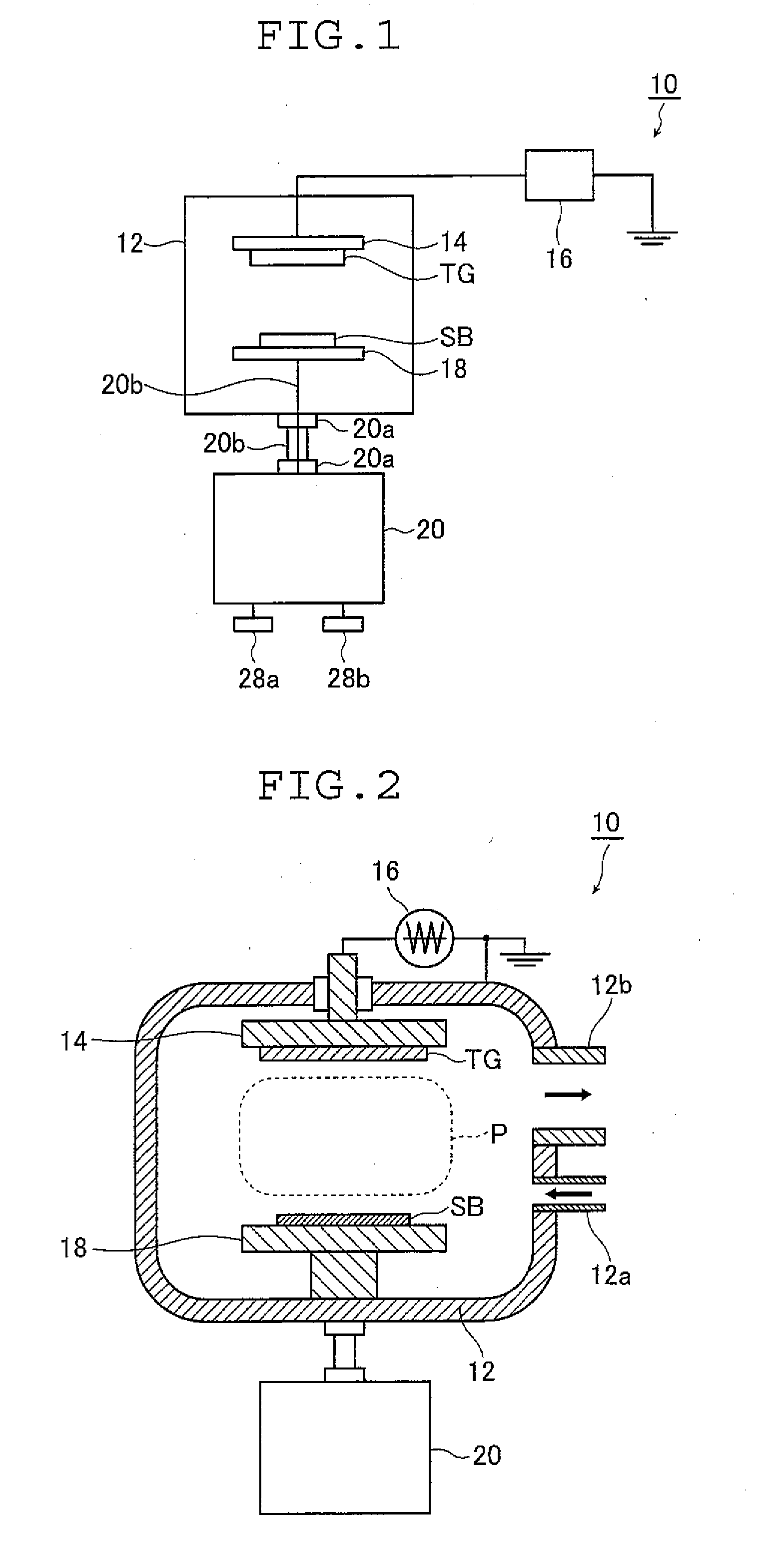
[0230]Model STV 4320 of Shinko Seiki Co., Ltd. was used as the sputtering apparatus 10 shown in FIGS. 1 and 2. In this sputtering apparatus 10, the substrate holder 18 was of such a design as to permit selection between the grounded state and a floating state. The RF power source 16 was capable of applying RF power of up to 1 kW.

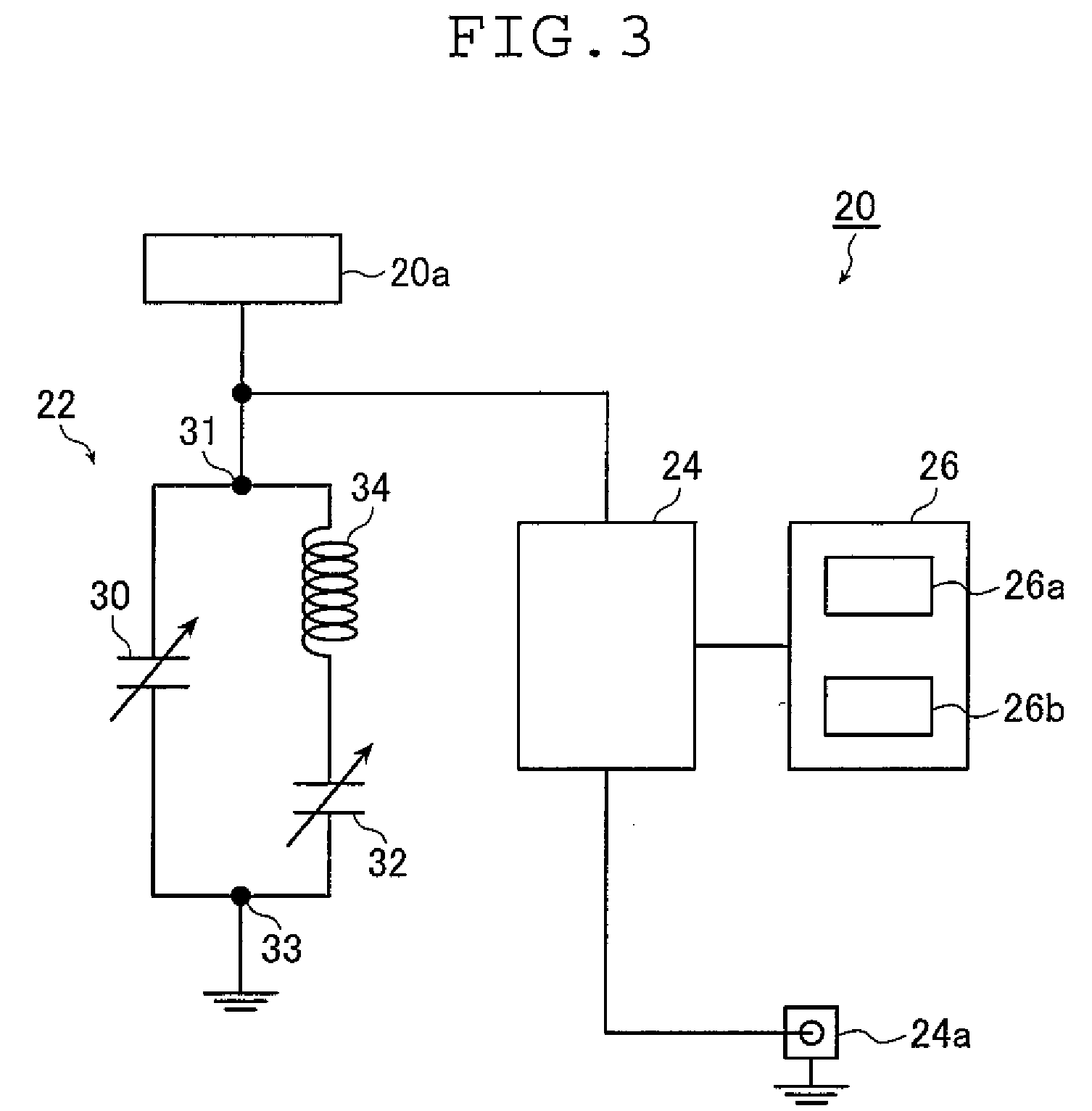
[0231]The sputtering apparatus 10 shown in FIGS. 1 and 2 used the impedance adjusting circuit 20 as shown in FIG. 3 and it was connected to the substrate holder 18.

[0232]A 4-inch size of sintered compact with the composition Pb1.3Zr0.52Ti0.48Ox was used as the target material TG. The substrate SB measured 5 cm by square and had Ti and Ir preliminarily formed in respective thicknesses of 10 nm and 150 nm on a Si wafer.

[0233]The target material TG and the substrate SB were spaced apart by 60 mm.

[0234]With the substrate temperature set at 525° C., a gas mixture of Ar and O2 (2.5%) was introduced to deposit a PZT film at 0.5 Pa.

[0235]With the substrate ...

Example

Comparative Example 1

[0240]An experiment was conducted as in Example 1, except that the target material TG and the substrate SB were spaced apart by 12 cm and that the substrate potential Vf was adjusted at 10 or 11 volts.

[0241]The results are shown in Table 2 below.

TABLE 2Vf(V)Structure of deposited filmCondition 710pyrochlore phase + perovskite phaseCondition 810pyrochlore phase + perovskite phaseCondition 910pyrochlore phase + perovskite phaseCondition 1010pyrochlore phase + perovskite phaseCondition 1111pyrochlore phase + perovskite phase

[0242]As is clear from Table 2, the substrate potential Vf remained substantially unchanged in Comparative Example 1, so the structures of the deposited films were virtually the same. As the result, the film quality was obviously impossible to control.

[0243]When the distance between the substrate SB and the target material TG was great, the substrate potential Vf did not change probably because the substrate SB was too far away from the place wh...

Example

Example 2

[0244]More than one batch of film deposition was performed for two cases, one where the substrate potential Vf was adjusted and the other where it was not. The results are shown in Table 3 below.

TABLE 3VfVf(adjusted)(not adjusted)Batch 11010Batch 51011Batch 101013CleanedBatch 11010

[0245]As is clear from Table 3, the potential Vf of the substrate SB could be held constant in Example 2 by adjusting it but when it was not adjusted, the potential of the substrate SB changed gradually. In the absence of adjustment, an insulating film may have formed near the substrate holder 18 or on the side walls of the-vacuum vessel 12, causing the plasma state and, hence, the potential of the substrate SB to change. On the other hand, adjustment must have enabled film deposition to occur at a constant potential.

[0246]Therefore, by adjusting it, the substrate potential Vf can be held at a constant value or within a predetermined range to prevent a change in film quality, thus enabling piezoel...


PUM

PropertyMeasurementUnit
Distanceaaaaaaaaaa
Distanceaaaaaaaaaa
Piezoelectricityaaaaaaaaaa

Abstract

The sputtering apparatus includes a vacuum vessel, a sputter electrode placed within the vacuum vessel to hold a target material to be sputtered, a radio frequency power source for applying radio frequency waves to the electrode, a substrate holder which is spaced from the electrode and on which a substrate is held, a thin film being to be deposited on the substrate from components of the target material, and an impedance adjusting circuit for adjusting a first impedance of the substrate holder. The impedance adjusting circuit has a first end directly set at a ground potential and has an impedance circuit which is adjustable for adjusting the first impedance, a second impedance of the impedance circuit is adjusted to thereby adjust the first impedance and, hence, a potential of the substrate.

Description

BACKGROUND OF THE INVENTION[0001]This invention relates to a sputtering apparatus and method, more particularly to a sputtering apparatus that deposits films by plasma-enhanced vapor-phase growth techniques, a sputtering method that uses the apparatus to deposit thin films such as insulating films (insulators) or dielectric films (dielectrics), insulating films or dielectric films such as piezoelectric films that are deposited by such sputtering apparatus and method, as well as piezoelectric devices that use the piezoelectric films, and an ink-jet apparatus that is equipped with the piezoelectric devices.[0002]Conventionally, thin films such as piezoelectric films, insulating films and dielectric films are deposited by the sputtering method that deposits films by plasma-enhanced vapor-phase growth techniques or a sputtering apparatus that uses this method. In such sputtering method and apparatus, high-energy Ar ions or other plasma ions that are produced by plasma discharge in high ...

Claims


Application Information

Patent Timeline
IPC IPC(8): C23C14/00B41J2/045H01L41/00B41J2/14B41J2/16C23C14/34H01L41/09H01L41/18H01L41/22H01L41/316H01L41/39
CPCB41J2/161B41J2/1646H01L41/316H01J37/34H01J37/3444C23C14/088H10N30/076
Inventor FUJII, TAKAMICHINAONO, TAKAYUKI
Owner FUJIFILM CORP
Why Eureka
Try Eureka