

Semiconductor device and method of manufacturing the same
- Summary
- Abstract
- Description
- Claims
- Application Information
AI Technical Summary
Benefits of technology
Problems solved by technology
Method used
Image

Examples
Embodiment Construction
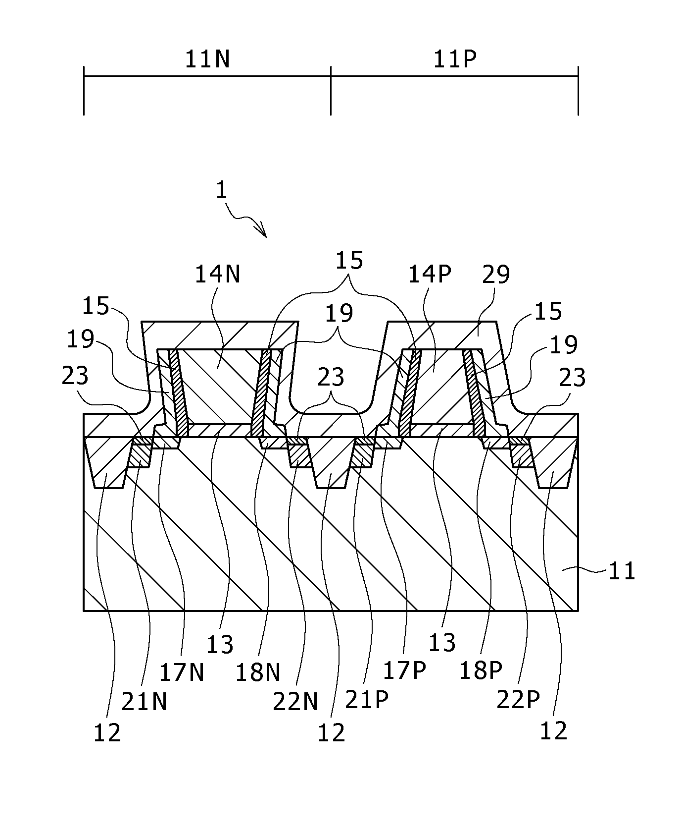
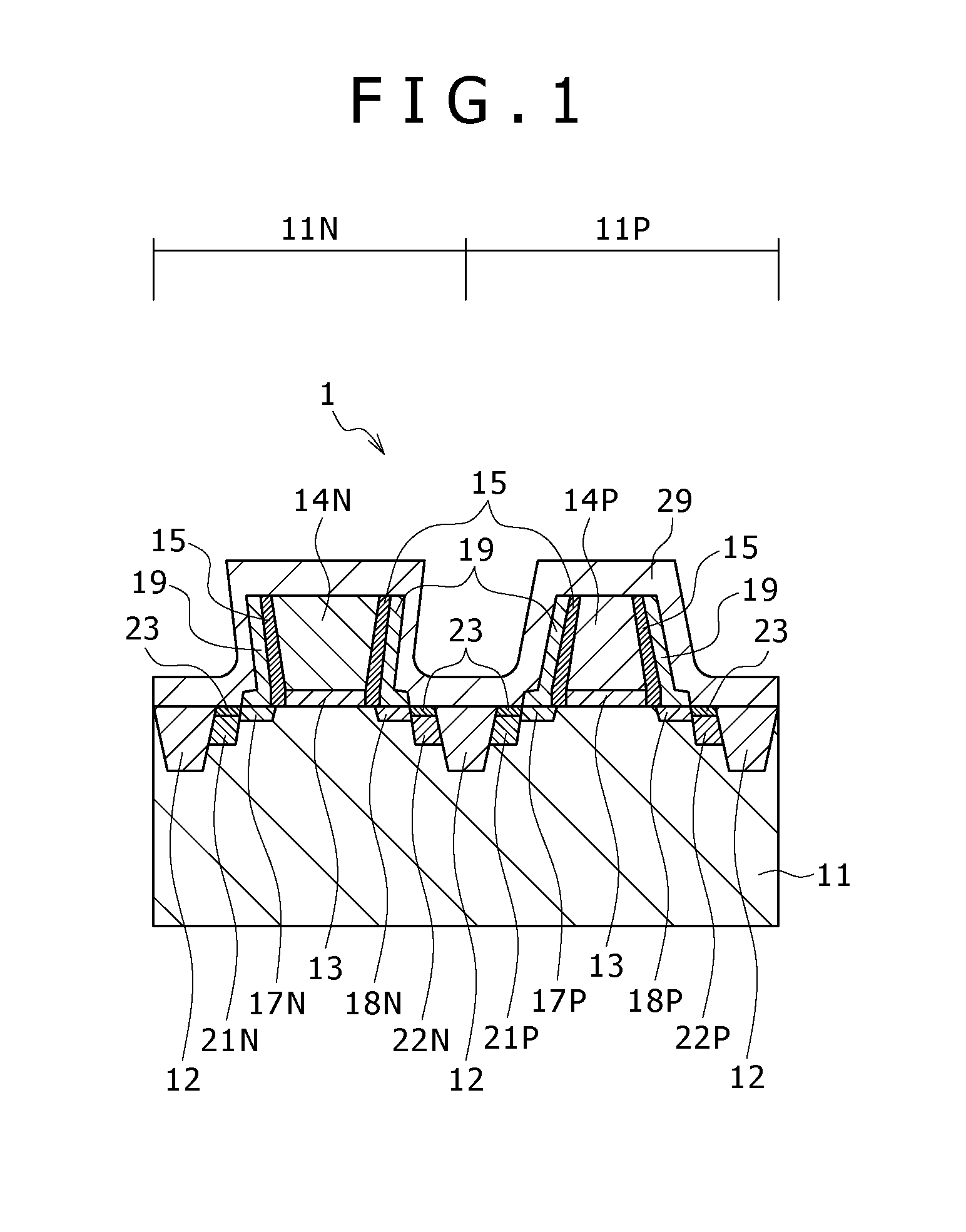
[0026]Now, an embodiment of the semiconductor device based on the present invention will be described below referring to a schematic configuration sectional view shown in FIG. 1.
[0027]As shown in FIG. 1, device isolation regions 12 for isolating an N-type FET (for example, N-type MOSFET) formation region 11N and a P-type FET (for example, P-type MOSFET) formation region 11P from each other are formed in a semiconductor substrate 11. As the semiconductor substrate 11, for example, a silicon substrate is used. Naturally, a compound semiconductor substrate can also be used. Optimum channel impurities are introduced respectively into the formation regions 11N and 11P.
[0028]The semiconductor substrate 11 is provided with a gate electrode 14N and a gate electrode 14P, with a gate insulator film 13 interposed therebetween. The gate insulator film 13 includes, for example, a high dielectric constant film, examples of which include a hafnium nitride silicate (HfSiON) film.
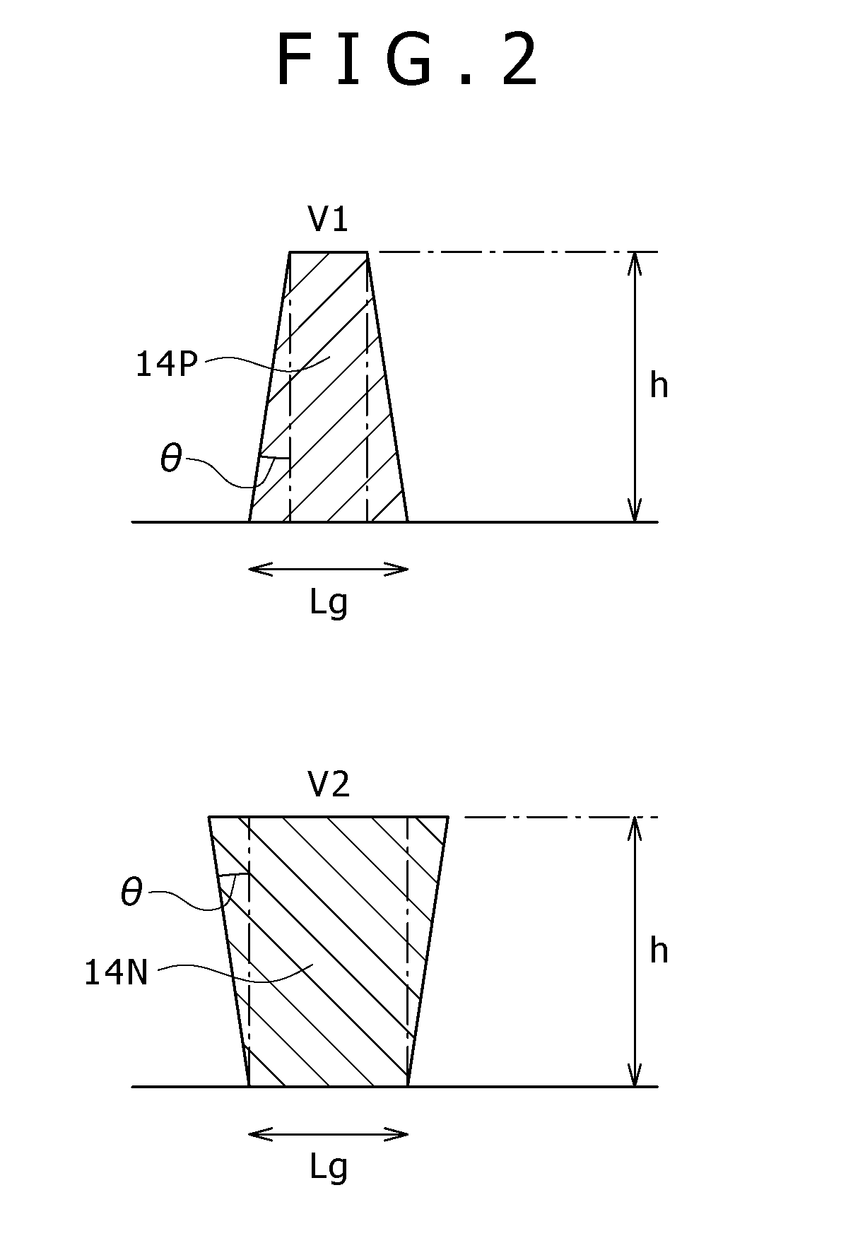
[0029]The gate elec...
PUM
 Abstract
Description
Claims
Application Information