Precharge controlling method and display device using the same

a display device and control method technology, applied in the direction of electric variable regulation, process and machine control, instruments, etc., can solve the problems of high contrast of the entire panel picture, error between the optimal coupling voltage value and the coupling voltage value supplied to the display device, and image is darkly displayed in the entire panel surface. , to achieve the effect of shortening the precharge time period, and reducing the precharge error

Active Publication Date: 2009-03-05
JAPAN DISPLAY WEST
View PDF12 Cites 17 Cited by
  • Summary
  • Abstract
  • Description
  • Claims
  • Application Information

AI Technical Summary

Benefits of technology

[0035]With the display device according to the another embodiment of the present invention, the output voltage from the output circuit is fed back to the output circuit through the comparator, which results in that the output voltage from the output circuit is properly precharged, thereby making it possible to output the proper voltage having the necessary level right after start of a normal operation. That is to say, it is possible to reduce the precharge error during the precharge operation until the optimal coupling voltage is reached.
[0036]According to the precharge controlling method of the embodiment of the present invention, the precision for the precharge operation until the proper voltage having the necessary level is reached in the activation phase can be enhanced, thereby making it possible to shorten the precharge time period in the voltage generating circuit for outputting the proper voltage having the necessary level. As a result, it is possible to accelerate the start-up of the normal operation.
[0037]According to the precharge controlling method of the embodiment of the present invention, the bias current in the output circuit is controlled through the voltage-current feedback circuit, thereby making it possible to further widen the dynamic range of the output voltage in the output circuit.
[0038]According to the display device of the another embodiment of the present invention, in the voltage generating circuit for outputting the proper coupling voltage used to drive the coupling capacitor of the pixel portion, the precision for the precharge operation until the proper coupling voltage is reached in the activation phase can be enhanced, thereby making it possible to shorten the precharge feedback. As a result, it is possible to accelerate the start-up of the normal operation of the display device.

Problems solved by technology

As a result, in an initial stage of start of the effective display for the pixel, an error occurs between the optimal coupling voltage value and the coupling voltage value supplied to the display device.
This error causes a problem that for example, in an initial stage of the activation, a contrast of the entire panel picture becomes high, and contrary, an image is darkly displayed in the entire panel surface.
The reason for this is because when only one of the capacitor Cin on the input side or the output load capacitor Cout is precharged, an operating point after completion of the precharge control does not agree with that during the normal operation, so that an output error may occur.

Method used


Image

  • Precharge controlling method and display device using the same
  • Precharge controlling method and display device using the same
  • Precharge controlling method and display device using the same

Examples


first embodiment

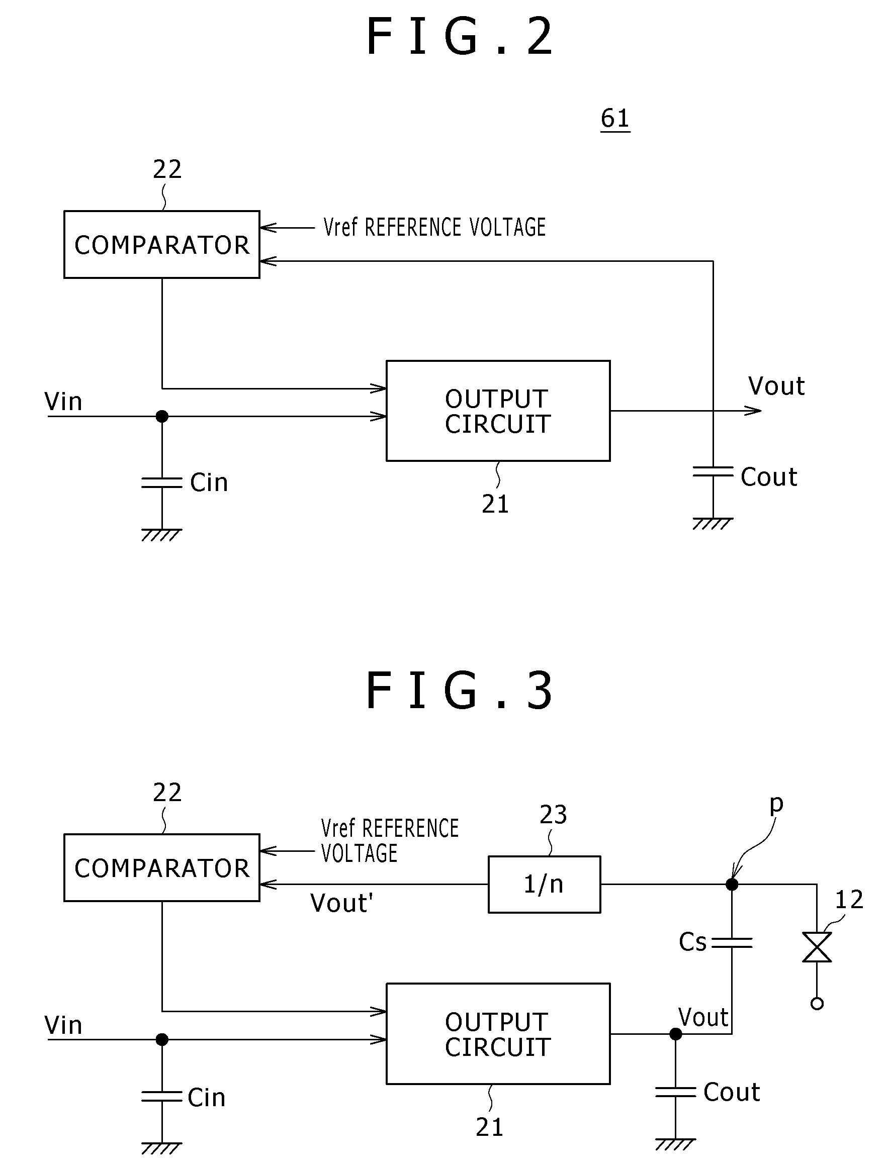
[0061]FIG. 2 is a block diagram, partly in circuit, showing a configuration of a voltage generating circuit 61 in a liquid crystal display device according to the present invention. The voltage generating circuit 61 in the liquid crystal display device according to this embodiment includes an output circuit 21 and a comparator 22. In this case, the comparator 22 compares an output voltage Vout from the output circuit 21 with a reference voltage Vref, and feeds an output voltage about a judgment result based on the comparison back to one input side of the output circuit 21. The low-pass filter 4 shown in FIG. 17 has the capacitor Cin. The capacitor Cin corresponds to an input capacitor Cin in the output circuit 21 shown in FIG. 2. An input voltage Vin is inputted to the other input terminal of the output circuit 21. Also, an output capacitor Cout is connected to an output side of the output circuit 21.

[0062]Here, although the details of a system for determining the reference voltage ...

second embodiment

[0072]FIG. 5 is a block diagram, partly in circuit, showing a configuration of a voltage generating circuit in a liquid crystal display device according to the present invention.

[0073]When in the block configuration shown in FIG. 2, the output circuit 21 is configured in the form of the general source follower circuit, a relationship of Expression (2) is established:

Vout=Vin+|Vgs(ID)|  (2)

[0074]Where Vgs (ID) is a gate to source voltage of the drive transistor TP1, and differs depending on the conditions such as the bias current ID caused to flow through the drive transistor TP1, the manufacture dispersion and the temperature. Therefore, when the constant voltage which is uniform with respect to the output voltage Vout is applied as the input voltage Vin, the precharge error becomes easy to occur. In other words, even when only the output side of the output circuit 21 is charged to have the necessary voltage, the output voltage generates the precharge error so as to follow the input...

third embodiment

[0110]FIG. 11 is a block diagram, partly in circuit, showing a configuration of a voltage generating circuit in a liquid crystal display device according to the present invention.

[0111]As previously stated, when the output circuit 21 is configured in the form of the general source follower circuit, the relationship given by Expression (2) is established. In this case, there is the necessity for quantitatively determining ID (the drain current caused to flow through the drive transistor TP1) in Expression (2). In general, there is a method of supplying a bias current from a current source transistor. The current source transistor means a constant current source transistor which is configured so as to cause a bias current to flow therefrom in accordance with a suitable bias current applied to a gate of a MOS transistor, for example, a p-channel transistor.

[0112]However, when longitudinally stacked current source transistors are used in the source follower (the source follower composed...


PUM


Abstract

An embodiment of the invention provides a precharge controlling method, including the steps of: providing a voltage generating circuit with an output circuit for outputting a voltage having a necessary level, and a comparator; judging an output voltage from the output circuit in the comparator during a precharge time period, and feeding back an output signal from the comparator to the output circuit; and controlling a precharge voltage until the voltage having the necessary level outputted from the output circuit is reached.

Description

CROSS REFERENCES TO RELATED APPLICATIONS[0001]The present invention contains subject matter related to Japanese Patent Application JP 2007-227169 filed in the Japan Patent Office on Aug. 31, 2007, the entire contents of which being incorporated herein by reference.BACKGROUND OF THE INVENTION[0002]1. Field of the Invention[0003]The present invention relates to a precharge controlling method, and a display device using the same.[0004]2. Description of Related Art[0005]A capacitive coupling drive system is known as a system for driving a display device, for example, a liquid crystal display device. In the liquid crystal display device using the capacitive coupling drive system, pixel portions each of which is composed of a switching element, a liquid crystal pixel cell, and a coupling capacitor Cs are formed so as to correspond to intersection portions in which scanning lines and signal lines intersect with each other, respectively. In this case, an offset voltage is applied as a poten...

Claims


Application Information

Patent Timeline
Patent Type & Authority Applications(United States)
IPC IPC(8): H05B37/02G05F1/10G05F1/00
CPCG05F1/56G09G3/3233G09G3/3655G09G2300/0876G09G2330/028G09G2320/0233G09G2320/0252G09G2320/041G09G2330/021G09G2310/0251G02F1/133G09G3/20G09G3/36
Inventor NAKAO, HIROSHI
Owner JAPAN DISPLAY WEST
Why Eureka
Try Eureka