Check patentability & draft patents in minutes with Patsnap Eureka AI!

Non-inverting amplifier circuit and optical switch driver circuit

a technology of amplifier circuit and driver circuit, which is applied in the direction of amplifiers, amplifiers with semiconductor devices only, amplifiers, etc., can solve the problems of light leakage, crosstalk of light, slow rising and falling waveform, etc., and achieve the effect of reducing the effect of internal delay and high speed

Inactive Publication Date: 2009-03-05
FUJITSU LTD
View PDF3 Cites 12 Cited by
  • Summary
  • Abstract
  • Description
  • Claims
  • Application Information

AI Technical Summary

Benefits of technology

[0034]Embodiments of the present invention may solve or reduce one or more of the above-described problems.
[0036]According to one embodiment of the present invention, a non-inverting amplifier circuit and an optical switch driver circuit are provided that are capable of driving a load at high speed by reducing the effect of the internal delay of the load.
[0040]According to one aspect of the present invention, it is possible to reduce the effect of the internal delay of a load and drive the load at high speed.

Problems solved by technology

However, there is leakage of light even in the OFF state, and this causes crosstalk of light in the multiplexing couplers 12-1 through 12-n.
However, even if the speed is high on the driver circuit side, there is an existing time constant of approximately 3 ns due to the internal delay of the SOA chip.
This time constant serves as an impediment to high-speed switching, thus resulting in a slow rising and falling waveform.
According to this method, there is a problem in the stability of the driver circuit because oscillation may occur depending on the type of the transistor Q1 and the output of the transistor Q1 may be current overload.
As a result, because of occurrence of the ringing having amplitude substantially greater than the 1.5 V drive voltage in the output voltage waveform of the transistor Q1 and occurrence of voltage exceeding 0.65 V in the voltage waveform after passing through the delay equivalent circuit 32, there is a problem in that the extinction ratio characteristic of approximately 58 dB between the ON state and OFF state of the SOA gate-type optical switch in FIG. 7 cannot be satisfied.

Method used


Image

  • Non-inverting amplifier circuit and optical switch driver circuit
  • Non-inverting amplifier circuit and optical switch driver circuit
  • Non-inverting amplifier circuit and optical switch driver circuit

Examples


first embodiment

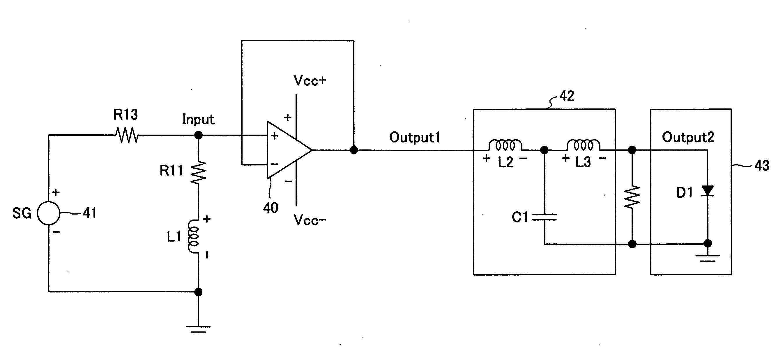
[0062]FIG. 14 is a circuit diagram showing an optical switch driver circuit according to a first embodiment of the present invention. This optical switch driver circuit is a preemphasis type. FIG. 15 is a waveform chart for illustrating the rising operating speed of the circuit shown in FIG. 14. FIG. 16 is a waveform chart for illustrating the falling operating speed of the circuit shown in FIG. 14.

[0063]FIG. 14 shows a circuit that drives an SOA gate-type optical switch, using a high-speed operational amplifier 40 that has an output current capacity of 300 mA or more and has a settling time of approximately 2 ns. The operational amplifier 40 has its output connected to its inverting input so as to form a voltage follower circuit.

[0064]A resistor R13 is connected between the positive terminal of a signal generator (SG) 41 and the non-inverting input of the operational amplifier 40. The non-inverting input of the operational amplifier 40 is grounded through a terminating resistor R11...

second embodiment

[0070]FIG. 17 is a circuit diagram showing an optical switch driver circuit according to a second embodiment of the present invention. This optical switch driver circuit is a preemphasis type. FIG. 18 is a waveform chart for illustrating the rising operating speed of the circuit shown in FIG. 17. FIG. 19 is a waveform chart for illustrating the falling operating speed of the circuit shown in FIG. 17. In FIG. 17, the same elements as those of FIG. 14 are referred to by the same reference numerals.

[0071]FIG. 17 shows a circuit that drives an SOA gate-type optical switch, using the high-speed operational amplifier 40 that has an output current capacity of 300 mA or more and has a settling time of approximately 2 ns. The operational amplifier 40 has its output connected to its inverting input so as to form a voltage follower circuit.

[0072]A resistor R23 and a capacitor C12 are connected in parallel between the positive terminal of the signal generator 41 and the non-inverting input of t...


PUM


Abstract

A non-inverting amplifier circuit is disclosed that includes an operational amplifier and a preemphasis circuit connected between the operational amplifier and a signal source. The preemphasis circuit is configured to compensate for the internal delay of a load connected to the output of the operational amplifier by emphasizing a high-frequency component of a signal fed from the signal source.

Description

BACKGROUND OF THE INVENTION[0001]1. Field of the Invention[0002]The present invention relates generally to non-inverting amplifier circuits and optical switch driver circuits, and more particularly to a non-inverting amplifier circuit and an optical switch driver circuit that improve the sound quality of an audio signal having partly thinned-out spectrum components by performing interpolation on the thinned-out spectrum components.[0003]2. Description of the Related Art[0004]There has been a demand for high-speed and large-capacity optical communications devices toward future construction of a multimedia network. Research and development has been carried out on an optical packet switching system using a high-speed optical switch of an order of magnitude of nanoseconds (ns) as a system for achieving this high speed and large capacity.[0005]The SOA (Semiconductor Optical Amplifier) gate-type optical switch, which is a device capable of high-speed switching of an order of magnitude of ...

Claims


Application Information

Patent Timeline
IPC IPC(8): H03F3/04
CPCH03F1/565
Inventor UENO, TOMOHIRONOGUCHI, MASAJIKAI, YUTAKAYOSHIDA, SETSUO
Owner FUJITSU LTD
Features
  • R&D
  • Intellectual Property
  • Life Sciences
  • Materials
  • Tech Scout
  • Unparalleled Data Quality
  • Higher Quality Content
  • 60% Fewer Hallucinations
Learn More