MOS device with schottky barrier controlling layer

a technology of schottky barrier and mos device, which is applied in the direction of diodes, radiation controlled devices, semiconductor devices, etc., can solve the problems of efficiency loss, limited cell per unit area, and limited channel length l,

Active Publication Date: 2009-03-12
ALPHA & OMEGA SEMICON LTD
View PDF62 Cites 54 Cited by
  • Summary
  • Abstract
  • Description
  • Claims
  • Application Information

AI Technical Summary

Problems solved by technology

However, the channel length L is typically limited because of the punch-through phenomenon.
The number of cells per unit area is limited by manufacturing technology and by the need to make a good contact to both the source and body regions of the cell.
In some applications such as synchronous rectification, the stored charge and forward drop of the body diode also result in efficiency loss.
These factors together tend to limit the performance of DMOS power devices.

Method used


Image

  • MOS device with schottky barrier controlling layer
  • MOS device with schottky barrier controlling layer
  • MOS device with schottky barrier controlling layer

Examples


Embodiment Construction

[0012]The invention can be implemented in numerous ways, including as a process, an apparatus, a system, a composition of matter, a computer readable medium such as a computer readable storage medium or a computer network wherein program instructions are sent over optical or communication links. In this specification, these implementations, or any other form that the invention may take, may be referred to as techniques. A component such as a processor or a memory described as being configured to perform a task includes both a general component that is temporarily configured to perform the task at a given time or a specific component that is manufactured to perform the task. In general, the order of the steps of disclosed processes may be altered within the scope of the invention.

[0013]A detailed description of one or more embodiments of the invention is provided below along with accompanying figures that illustrate the principles of the invention. The invention is described in conne...


PUM


Abstract

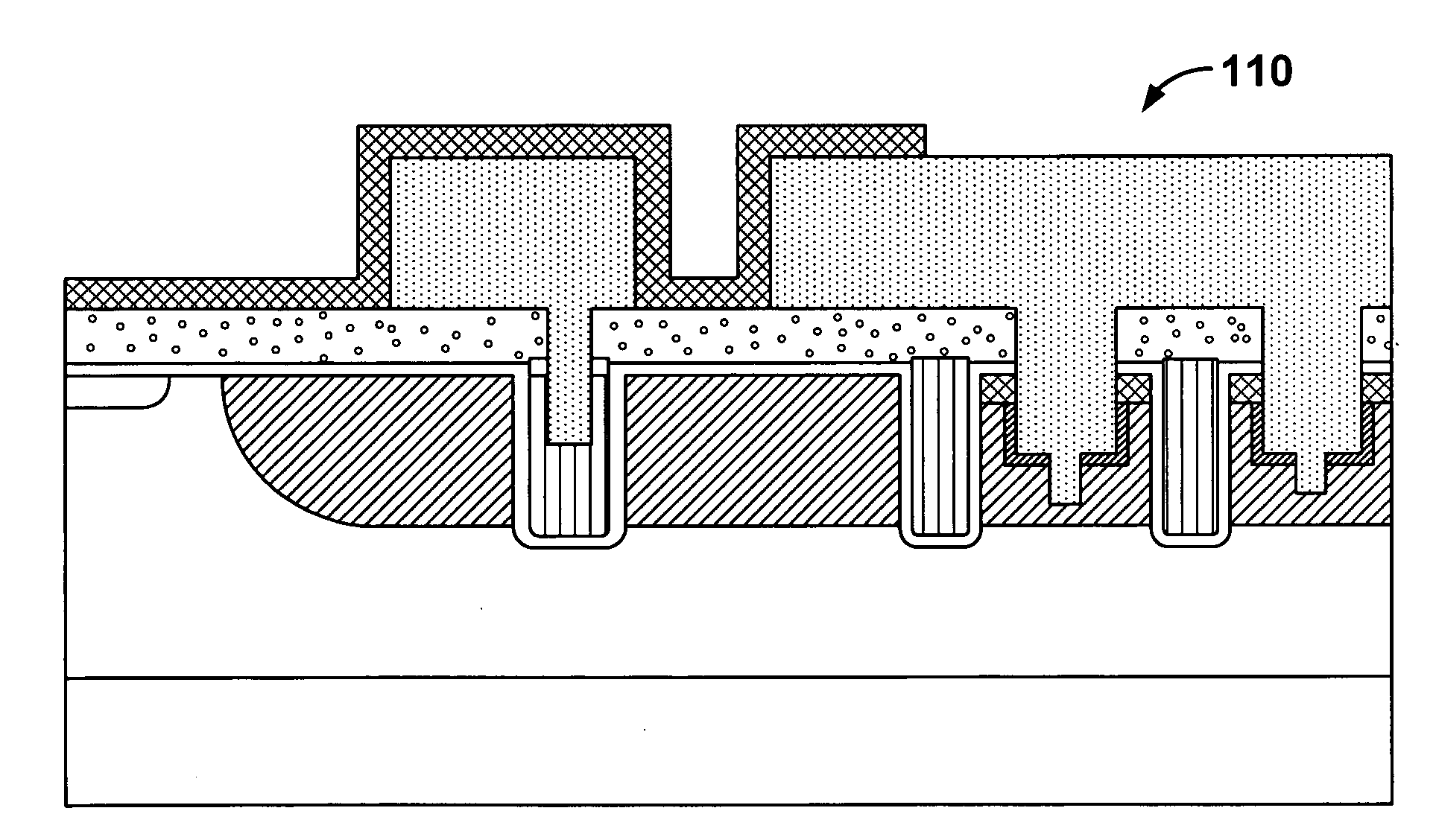
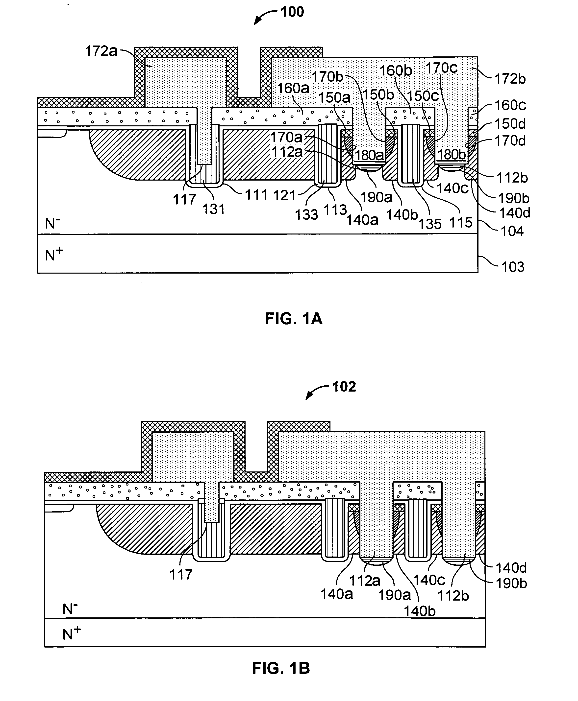
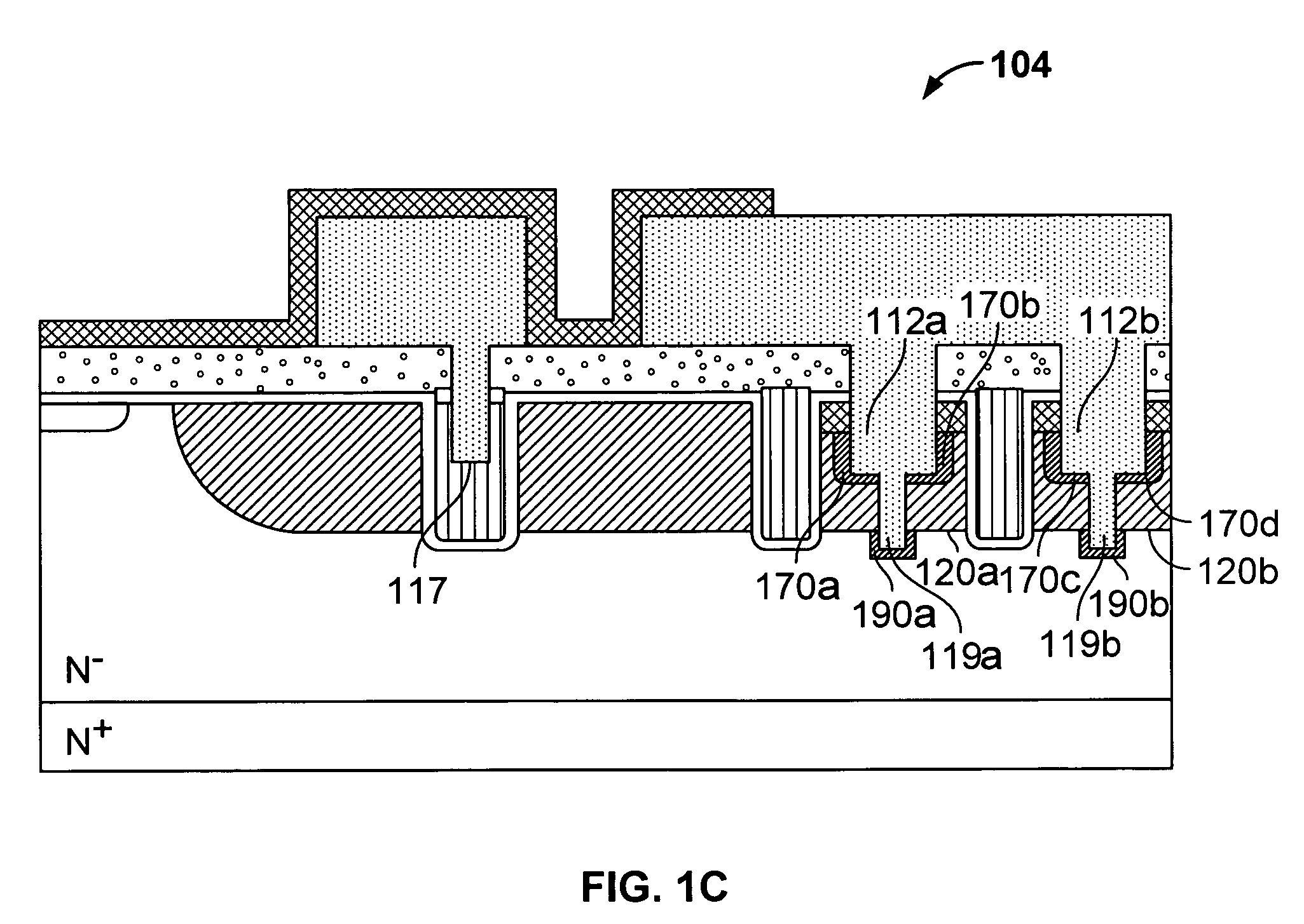
A semiconductor device is formed on a semiconductor substrate. The semiconductor device comprises a drain, an epitaxial layer overlaying the drain, and an active region. The active region comprises a body disposed in the epitaxial layer, having a body top surface, a source embedded in the body, extending from the body top surface into the body, a gate trench extending into the epitaxial layer, a gate disposed in the gate trench, an active region contact trench extending through the source and the body into the drain, an active region contact electrode disposed within the active region contact trench, wherein the active region contact electrode and the drain form a Schottky diode, and a Schottky barrier controlling layer disposed in the epitaxial layer adjacent to the active region contact trench.

Description

CROSS REFERENCE TO OTHER APPLICATIONS[0001]This application is a continuation in part of co-pending U.S. patent application Ser. No. 11 / 900,616 entitled POWER MOS DEVICE filed Sep. 11, 2007, which is incorporated herein by reference for all purposes, and which is a continuation of U.S. patent Ser. No. 11 / 056,346 entitled POWER MOS DEVICE filed Feb. 11, 2005, now U.S. Pat. No. 7,285,822, which is incorporated herein by reference for all purposes.BACKGROUND OF THE INVENTION[0002]Power MOS devices are commonly used in electronic circuits. Depending on the application, different device characteristics may be desirable. One example application is a DC-DC converter, which includes a power MOS device as a synchronous rectifier (also referred to as the low side FET) and another power MOS device as a control switch (also referred to as the high side FET). The low side FET typically requires a small on-resistance to achieve good power switch efficiency. The high side FET typically requires a ...

Claims


Application Information

Patent Timeline
Patent Type & Authority Applications(United States)
IPC IPC(8): H01L29/78H01L21/338
CPCH01L21/26586H01L29/66143H01L29/1095H01L29/165H01L29/41766H01L29/4236H01L29/456H01L29/47H01L29/66727H01L29/66734H01L29/7806H01L29/7811H01L29/7813H01L29/7809H01L29/8725H01L21/26513H01L29/41741H01L29/0623H01L29/1083
Inventor BHALLA, ANUPWANG, XIAOBINPAN, JIWEI, SUNG-PO
Owner ALPHA & OMEGA SEMICON LTD
Why Eureka
Try Eureka