Method and structures for accelerated soft-error testing

a technology of integrated circuits and methods, applied in the field of integrated circuits, can solve problems such as disposal problems, generation of errors, contamination of manufacturing and testing facilities,

Inactive Publication Date: 2009-03-12
GLOBALFOUNDRIES INC
View PDF18 Cites 65 Cited by
  • Summary
  • Abstract
  • Description
  • Claims
  • Application Information

AI Technical Summary

Benefits of technology

[0003]A first aspect of the present invention is an integrated circuit chip, comprising: a silicon substrate; a dielectric layer formed over the substrate; electrically conductive wires formed in the dielectric layer, the wires interconnecting semiconductor devices formed in the substrate into circuits; and an alpha particle emitting region in the integrated circuit chip proximate to one or more of the semiconductor devices.
[0004]A second aspect of the present invention is a method of fabricating an integrated circuit chip, comprising: forming a dielectric layer over a substrate; forming electrically conductive wires in the dielectric layer, the wires interconnecting semiconductor devices formed in the substrate into circuits; and forming an alpha particle emitting region in the integrated circuit chip proximate to one or more of the semiconductor devices.
[0005]A third aspect of the presen

Problems solved by technology

Soft-errors in integrated circuits are caused by ionizing radiation striking, for example, the silicon regions of field effect transistors in memory cells or latches and changing the charge level stored in the cell or latch causing a flip in state of the cell or latch and thus generating an error.
Some integrated circuits are bonded to ceramic substrates, which prevent using an external alpha-particle beam for soft-error testing since the beam often does not have the range r

Method used


Image

  • Method and structures for accelerated soft-error testing
  • Method and structures for accelerated soft-error testing
  • Method and structures for accelerated soft-error testing

Examples


first embodiment

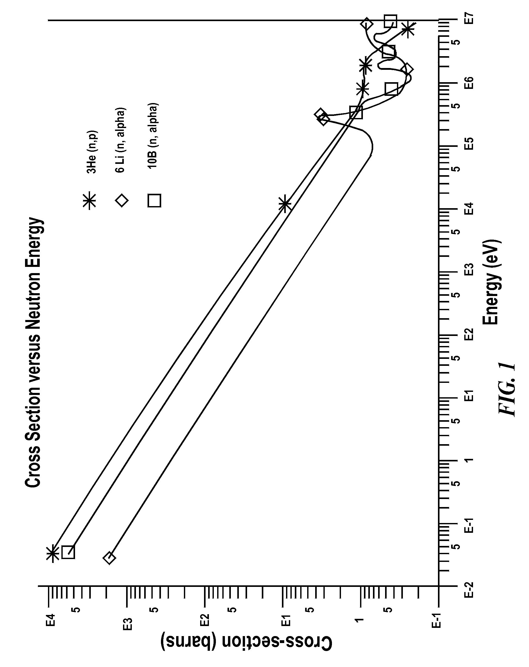
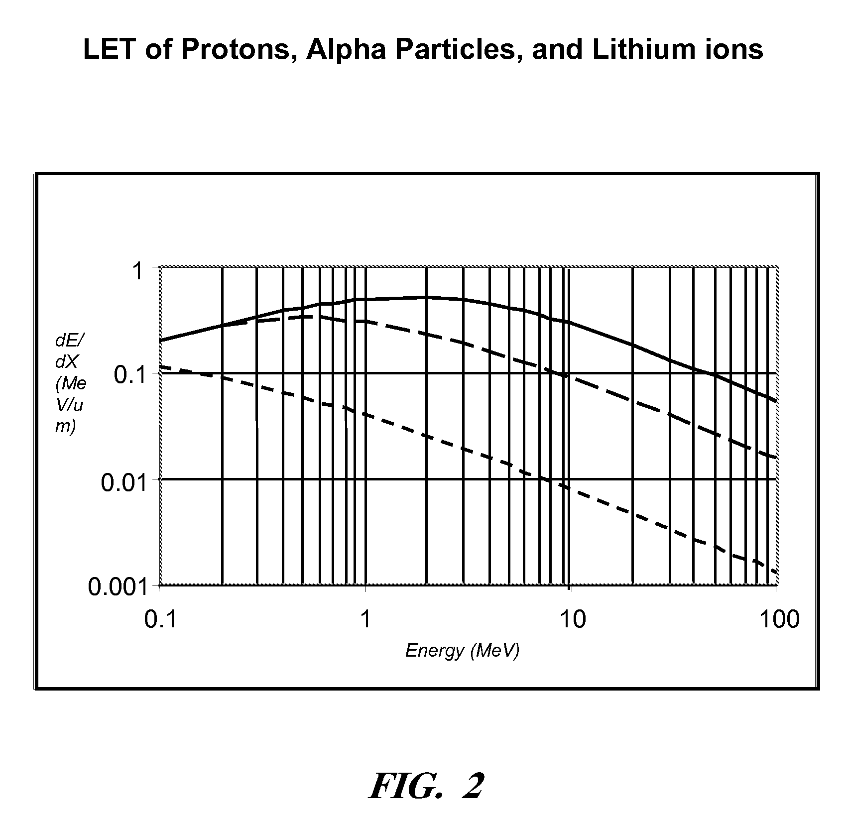
[0019]FIGS. 3A and 3B are cross-sectional drawings illustrating the present invention. In FIG. 3A, a silicon-on-insulator (SOI) substrate 100 comprises a buried oxide layer (BOX) 105 between an upper single-crystal silicon layer 110 and a supporting substrate 115. In one example, supporting substrate 115 is comprises silicon or single-crystal silicon. Substrate 100 is subjected to an ion implantation of 10B or 6Li ions 120 or both 10B and 6Li ions, which form an alpha particle emitting layer 125 in supporting substrate 115. The center of alpha emitting layer 125 is located a distance D from a top surface 127 of substrate 100. D is chosen such that, after all the heat cycles that substrate 100 is subjected to during fabrication of integrated circuits, alpha particle emitting layer 125 is close enough to upper silicon layer 110 for alpha particles emitted when the 10B or 6Li is struck by thermal neutrons to have range greater than the distance between the alpha particle layer and top ...

second embodiment

[0027]FIG. 4 is a cross-sectional drawing illustrating the present invention. FIG. 4 is similar to FIG. 3B except alpha particle emitting layer 125 has not been formed and the processing is shown after completion of wire formation in first ILD layer 160. In FIG. 4, first ILD layer 160 is subjected to the ion implantation of 10B or 6Li ions 120 or both 10B and 6Li ions, which form an alpha particle emitting layer 170 in ILD layer 160 and wires 165. Optionally, a patterned ion implantation mask may be formed over first ILD layer 160 to block ion-implantation of 10B or / and 6Li into certain wires 165 and regions of the first ILD layer. Since there are very few high temperature heat cycles after formation of first ILD layer 160, the 10B or / and 6Li will stay mainly within first ILD 160 and wires 165. After the ion implantation, additional ILD layers and wires may be formed to complete the integrated circuit chips.

[0028]When and integrated circuit chip containing alpha particle emitting la...

third embodiment

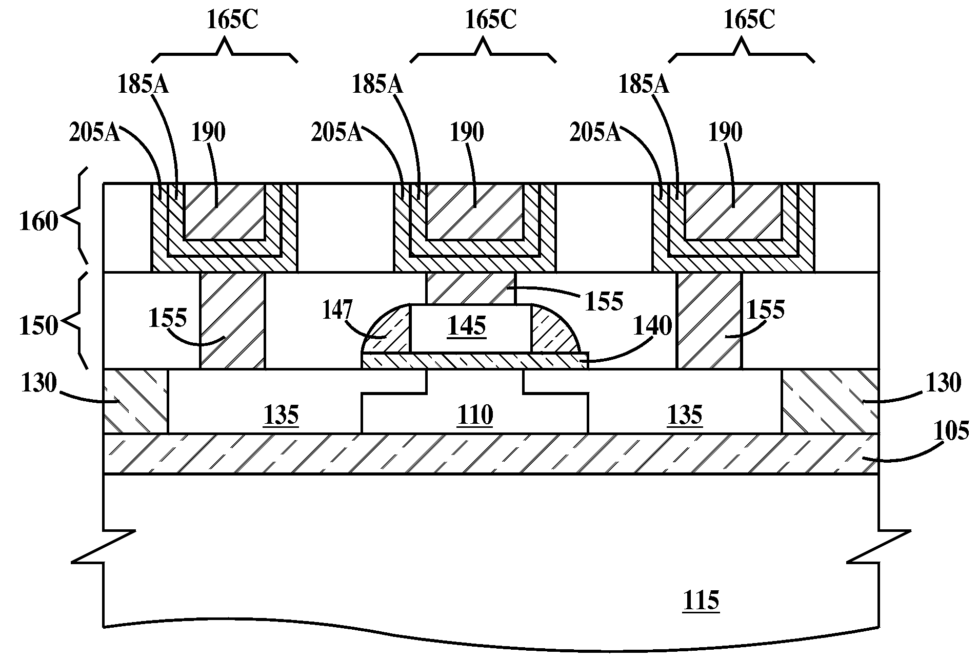
[0029]FIGS. 5A through 5C are cross-sectional drawing illustrating the present invention. FIG. 5A is similar to FIG. 3B up to formation of ILD layer 160. In FIG. 5A, trenches 175 are formed in ILD layer 160 and an electrically conductive conformal layer 180 is formed on the sidewalls and bottoms of trenches 175 and the top surface of ILD layer 160. Conformal layer 180 may be formed, for example, by sputter deposition. In one example, conformal layer 180 comprises, tantalum (Ta), tantalum nitride (TaN), titanium (Ti), titanium nitride (TiN) or combinations thereof. Alternatively, conformal layer 180 may be formed by chemical-vapor deposition (CVD).

[0030]In FIG. 5B a conformal doped seed layer 185 comprising copper (Cu) and 10B, Cu and 6Li or Cu, 10B and 6Li is formed by sputter deposition from a target comprised of Cu and 10B and / or 6Li. In sputter deposition, ions (e.g., argon ions) are directed to a target in vacuum chamber and particles of the target are ejected from the target by...


PUM


Abstract

An integrated circuit, method of forming the integrated circuit and a method of testing the integrated circuit for soft-error fails. The integrated circuit includes: a silicon substrate; a dielectric layer formed over the substrate; electrically conductive wires formed in the dielectric layer, the wires interconnecting semiconductor devices formed in the substrate into circuits; and an alpha particle emitting region in the integrated circuit chip proximate to one or more of the semiconductor devices. The method includes exposing the integrated circuit to an artificial flux of thermal neutrons to cause fission of atoms in the alpha particle emitting region into alpha particles and other atoms.

Description

FIELD OF THE INVENTION[0001]The present invention relates to the field of integrated circuits; more specifically, it relates to a method and structures for accelerated soft-error testing of integrated circuits.BACKGROUND OF THE INVENTION[0002]Soft-errors in integrated circuits are caused by ionizing radiation striking, for example, the silicon regions of field effect transistors in memory cells or latches and changing the charge level stored in the cell or latch causing a flip in state of the cell or latch and thus generating an error. The error state is removed the next time data are written into the cell or latch. Some integrated circuits are bonded to ceramic substrates, which prevent using an external alpha-particle beam for soft-error testing since the beam often does not have the range required to get through the packaging materials. For this reason, advanced methods of soft-error rate testing utilize highly radioactive alpha particle emitters within the underfill that might p...

Claims


Application Information

Patent Timeline
IPC IPC(8): H01L23/48G01R31/26H01L21/4763
CPCG01R31/2858G01R31/2881G01R31/31816H01L21/76825H01L21/84H01L23/53233H01L2924/0002H01L23/53238H01L27/1203H01L2924/00
Inventor GORDON, MICHAEL S.RODBELL, KENNETH P.TANG, HENRY H. K.
Owner GLOBALFOUNDRIES INC
Why Eureka
Try Eureka