Semiconductor integrated circuit

Inactive Publication Date: 2009-03-19
HITACHI LTD
View PDF3 Cites 8 Cited by
  • Summary
  • Abstract
  • Description
  • Claims
  • Application Information

AI Technical Summary

Benefits of technology

[0013]A clock skew, especially the clock skew generated in the chi

Problems solved by technology

Although a characteristics variation in a chip is one of the subjects discussed in JP-A-Hei4(1992)-076610, the variation in the divided region in clock skew generated by a uniform OCV (systematic component) in the LSI as shown in the non-patent r

Method used


Image

  • Semiconductor integrated circuit
  • Semiconductor integrated circuit
  • Semiconductor integrated circuit

Examples


first embodiment

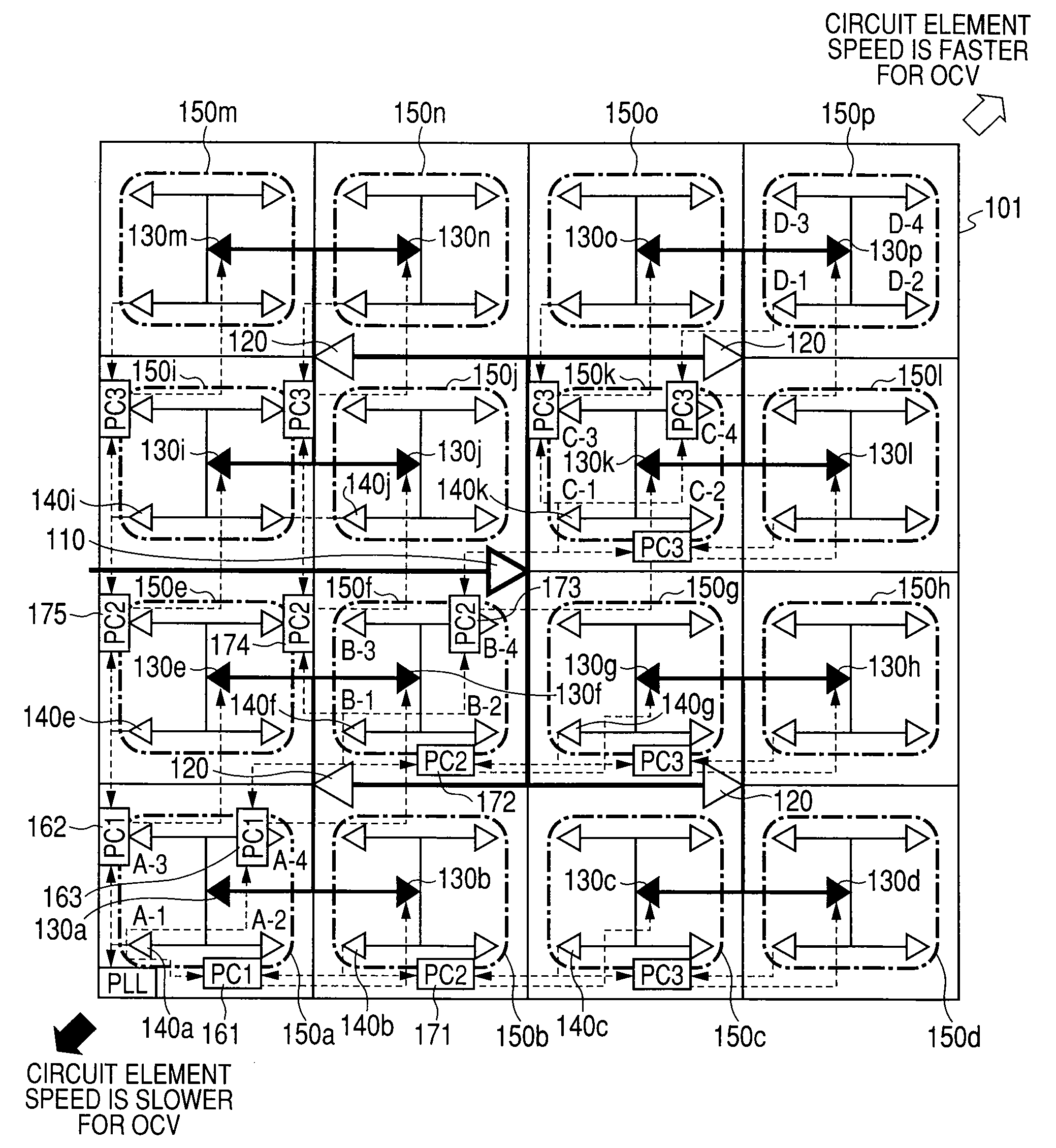
[0028]FIG. 1 shows the semiconductor integrated circuit of the first embodiment in accordance with the present invention. In the semiconductor chip 101 of this embodiment, a systematic OCV component is assumed to exist such that a circuit element speed becomes faster uniformly as the circuit element goes to the upper right from the lower left in the chip. Wherever an H tree clock branches, a clock distribution path branches and a lower layer clock tree (hereafter called a subordinate clock tree) distributes a clock to each of the divided regions. In the embodiment of FIG. 1, a first level clock driver 110 branches to four second level clock drivers 120, and also each of the second level clock drivers 120 branches to four third level clock drivers 130. The H tree clock of this embodiment is constituted so that the clock generated by the PLL with an end clock signal from the lower left in the semiconductor chip as a feedback clock is distributed over the entire chip to every circuit o...

second embodiment

[0065]The flow of design and production of the semiconductor integrated circuit in accordance with the present invention is shown in FIG. 12.

(Design Process)

[0066]An LSI is designed including a clock distributing circuit having a clock skew adjustment circuit shown in the first embodiment (S101). It is to be noted that elements such as macro cells and on-chip memories may be included by the LSI depending on the LSI to be designed. In this case, a clock distribution circuit is arranged and wired avoiding these elements (S102) Then, logical circuits other than the clocks are designed (8103).

(Production Process)

[0067]The LSI is produced based on the design data (S104) of LSI (S105). Sorting is performed by an LSI tester after production, and the judgment on quality either good or poor is performed (S106-S108). A clock skew adjustment circuit is operated, and the amount of delay of a variable delay circuit is set up to compensate the clock skew due to OCV etc., and the clock skew is min...


PUM


Abstract

The semiconductor integrated circuit includes a first subordinate clock tree 802 and a second subordinate clock tree 803, wherein a clock is delayed by a variable delay circuit 805 and inputted into the second subordinate clock tree 803 so that the phases are matched each other of the output clocks from the end clock drivers with the same position in respective trees, thereby reducing clock skew.

Description

CLAIM OF PRIORITY[0001]The present application claims priority from Japanese patent application JP 2007-240402 filed on Sep. 18, 2007, the content of which is hereby incorporated by reference into this application.FIELD OF THE INVENTION[0002]The present invention relates to a semiconductor integrated circuit, and especially to a delay time control circuit for a clock signal.BACKGROUND OF THE INVENTION[0003]In a large-scale integrated circuit (LSI) including a sequential circuit which operates in synchronization with a clock signal, the difference between two clock signals of different locations in the LSI (hereinafter called a clock skew) is one of the factors which reduce the operating frequency of the LSI directly. With the improvement in the speed of LSI, the ratio of the clock skew to one machine cycle is becoming large and the clock skew control and reduction are indispensable in order to achieve a high-speed operation of LSI. It is becoming impossible, therefore, to disregard ...

Claims


Application Information

Patent Timeline
IPC IPC(8): G06F1/04
CPCG06F1/10
Inventor FUKUOKA, TETSUYANAKAHARA, SHIGERUMOTOYOSHI, MINORU
Owner HITACHI LTD
Why Eureka
Try Eureka