Systems, Methods and Apparatuses for High Power Complementary Metal Oxide Semiconductor (CMOS) Antenna Switches Using Body Switching and External Component in Multi-Stacking Structure

a technology of complementary metal oxide semiconductors and antenna switches, which is applied in the field of antenna switches, can solve the problems of rf switch, current cmos technology presents a variety of difficulties, and cmos technology is not used for rf switches, and achieves the effects of high power handling capability, lower leakage current, and high power blocking capability

Active Publication Date: 2009-03-19
SAMSUNG ELECTRO MECHANICS CO LTD +1
View PDF21 Cites 51 Cited by
  • Summary
  • Abstract
  • Description
  • Claims
  • Application Information

AI Technical Summary

Benefits of technology

[0005]Embodiments of the invention may provide for CMOS RF switches, which may be referred to as a CMOS SPDT switch. According to an embodiment of the invention, the CMOS RF switch may be fabricated using a standard 0.18 um process, although other processes may be utilized without departing from the embodiments of the invention. In order to provide high-power handling capability in a multi-band operation (e.g., about 900 MHz, 1.9 G

Problems solved by technology

Two significant mobile application components—power amplifiers (PAs) and radio frequency (RF) switches—have not yet been commercially integrated into CMOS technology.
However, current CMOS technology presents a variety of difficulties for its application to RF switches.
In particular, CMOS material characte

Method used


Image

  • Systems, Methods and Apparatuses for High Power Complementary Metal Oxide Semiconductor (CMOS) Antenna Switches Using Body Switching and External Component in Multi-Stacking Structure
  • Systems, Methods and Apparatuses for High Power Complementary Metal Oxide Semiconductor (CMOS) Antenna Switches Using Body Switching and External Component in Multi-Stacking Structure
  • Systems, Methods and Apparatuses for High Power Complementary Metal Oxide Semiconductor (CMOS) Antenna Switches Using Body Switching and External Component in Multi-Stacking Structure

Examples


first embodiment

[0026]I. CMOS RF Antenna Switch

[0027]A CMOS RF antenna switch in accordance with an embodiment of the invention will be now be described with reference to FIGS. 1-3. It will be appreciated that while a particular embodiment of the CMOS RF antenna switch is illustrated in FIGS. 1-3, other variations of the illustrated CMOS RF antenna switch are available without departing from an embodiment of the invention.

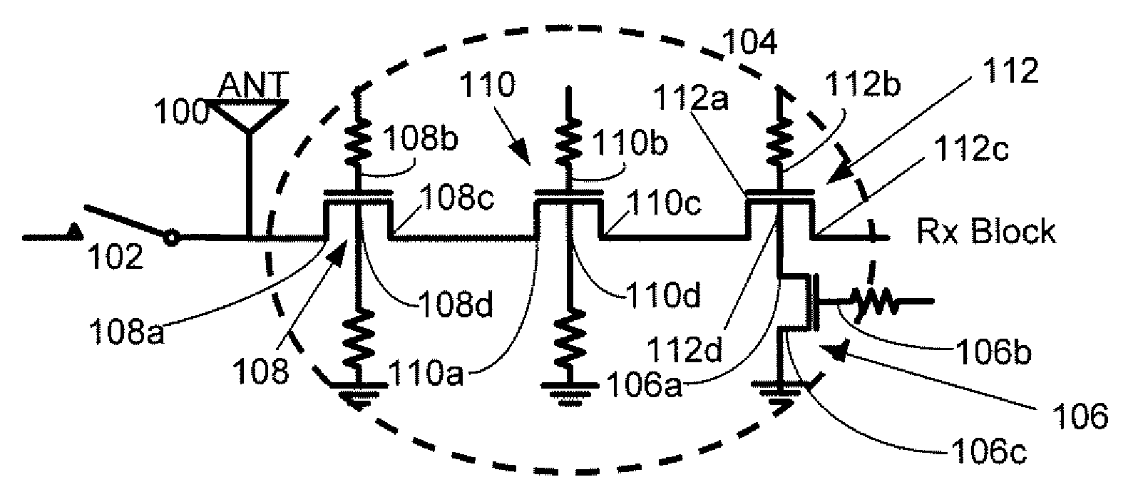
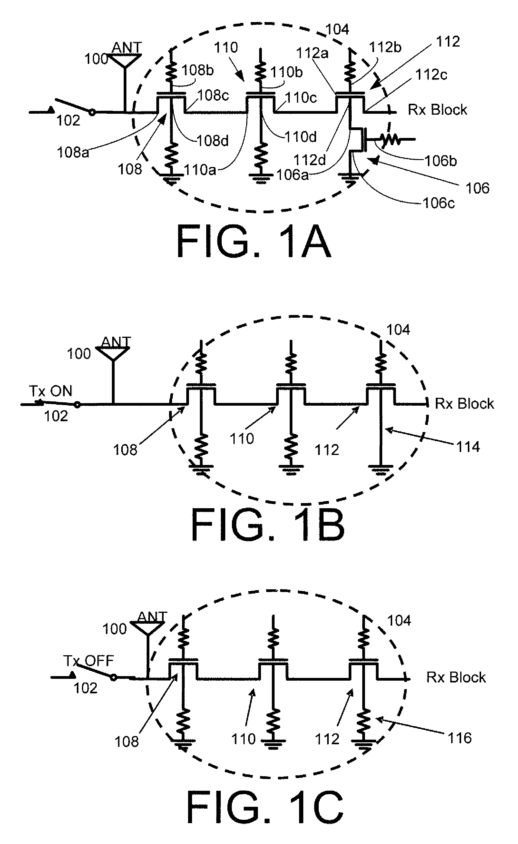
[0028]FIG. 1A illustrates a simplified CMOS RF antenna switch and its operation in accordance with an example embodiment of the invention. The CMOS RF antenna switch may include a transmit switch 102 and a receiver switch 104, in accordance with an example embodiment of the invention. Additionally, CMOS RF antenna switch may include an antenna 100 that is in communication with at least one of the transmit switch 102 and the receiver switch 104. According to an example embodiment of the invention, the antenna 100 may be a single multi-mode (e.g., RX and TX), multi-band antenna, alt...


PUM


Abstract

Embodiments of the invention may provide for a CMOS antenna switch, which may be referred to as a CMOS SPDT switch. The CMOS antenna switch may operate at a plurality of frequencies, perhaps around 900 MHz, 1.9 GHz and 2.1 GHz according to an embodiment of the invention. The CMOS antenna switch may include both a receiver switch and a transmit switch. The receiver switch may utilize a multi-stack transistor with body substrate switching and attachment of external capacitor between drain and gate to block high power signals from the transmit path as well as to maintain low insertion loss at the receiver path. Exemplary embodiments of the CMOS antenna switch may provide for 38 dBm P 0.1 dB at multi bands (e.g., 900 MHz, 1.8 GHz, and 2.1 GHz). In addition, −60 dBc second and third harmonic performance up to 30 dBm input, may be obtained according to example embodiments of the invention.

Description

FIELD OF THE INVENTION[0001]The invention relates generally to antenna switches, and more particularly, to CMOS (complementary metal oxide semiconductor) antenna switches.BACKGROUND OF THE INVENTION[0002]In the past decade, the wireless communication industry has experienced explosive growth, which has in turn accelerated the development of integrated circuit (IC) industry. In particular, in the IC industry, many mobile application systems like low noise amplifiers (LNAs), mixers, and voltage-controlled oscillators (VCOs) have been integrated into CMOS technology. Two significant mobile application components—power amplifiers (PAs) and radio frequency (RF) switches—have not yet been commercially integrated into CMOS technology.[0003]However, IC industry research is quickly moving towards power amplifier integrated into CMOS technology. For example, current research indicates that a CMOS power amplifier may be feasible and be able to provide a significant amount of power, perhaps up ...

Claims


Application Information

Patent Timeline
IPC IPC(8): H01Q3/24
CPCH03K17/063H03K17/102H04B1/48H03K2017/066H03K2217/0018H03K17/693H01P1/15H03K17/6871H03K17/00H04B1/44
Inventor AHN, MINSIKLEE, CHANG-HOCHANG, JAEJOONWOO, WANGMYONGKIM, HAKSUNLASKAR, JOY
Owner SAMSUNG ELECTRO MECHANICS CO LTD
Why Eureka
Try Eureka