Piezoelectric vibrating devices and methods for manufacturing same
- Summary
- Abstract
- Description
- Claims
- Application Information
AI Technical Summary
Benefits of technology
Problems solved by technology
Method used
Image

Examples
first embodiment
of Method for Manufacturing Tuning-Fork Type Crystal Vibrating Devices
[0051]In this embodiment, by simultaneously etching the profile outlines and the first groove regions 27, the etching (and overall processing) time is reduced compared to conventional processes. Also, shape variations in manufacturing lots of devices are reduced.
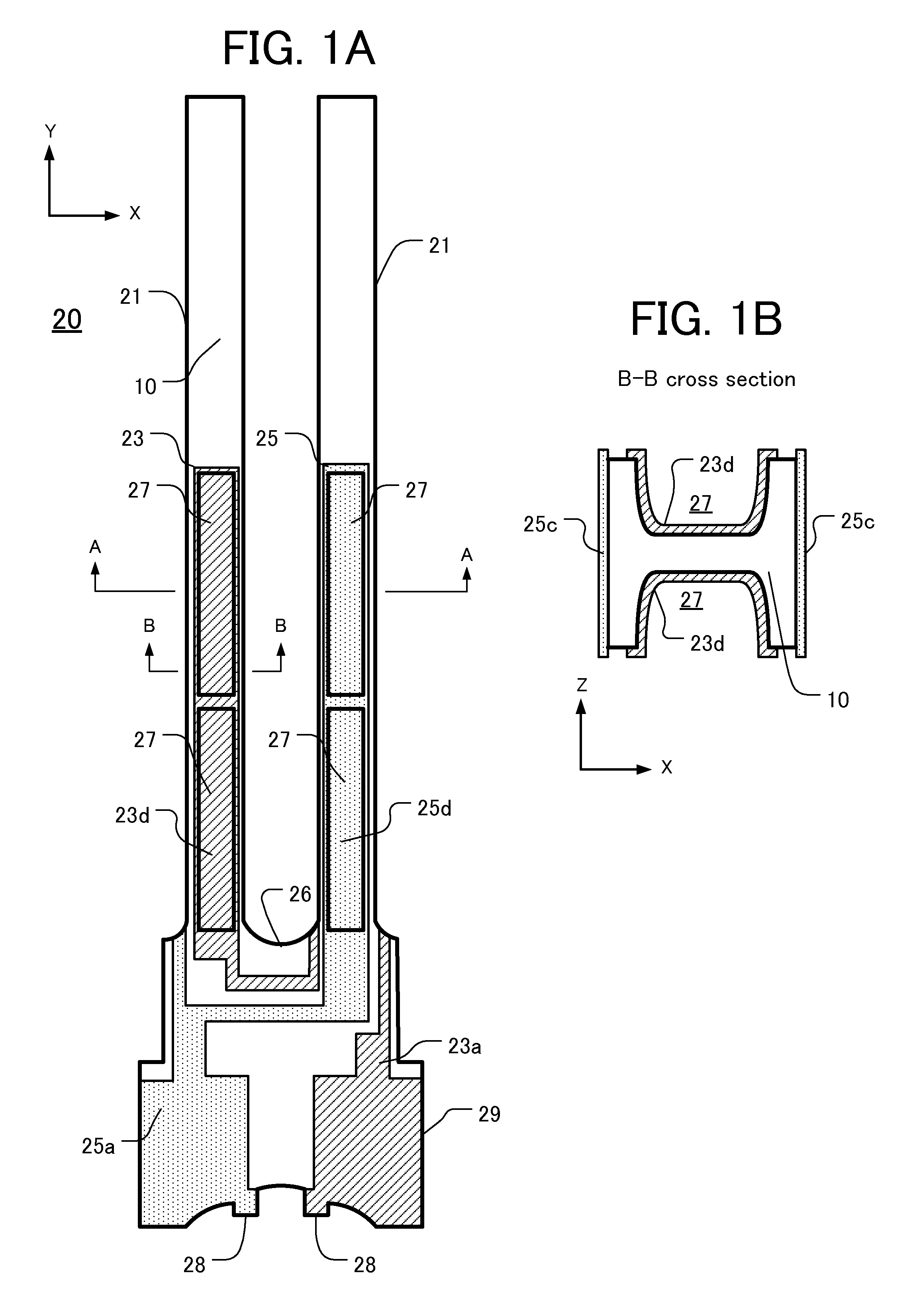
[0052]FIGS. 3 and 4 are respective flow-charts of a method for forming the profile outline and the first groove regions 27 of the tuning-fork type crystal vibrating devices 20. The respective figures to the right of the flow-chart steps are elevational sections, along the line A-A in FIG. 1A, depicting the result of the step.
[0053]In step S111 a single-crystal wafer 10 is prepared. Then, a metal film 32 is formed, by sputtering or other suitable deposition technique, on the entire surface (both sides) of the wafer 10. It is difficult to form gold (Au) or silver (Ag) directly on a piezoelectric wafer, so a chrome (Cr), nickel (Ni), or titanium (Ti) layer is...
second embodiment
of Method for Manufacturing Tuning-Fork Type Crystal Vibrating Devices
[0063]The process of this embodiment has fewer steps than the process of the first embodiment, allowing the tuning-fork type piezoelectric vibrating devices 20 to be formed in less time than achievable with the first embodiment. Key steps of this embodiment are shown in the flow-chart of FIG. 5. As in the figures corresponding to the first embodiment, figures on the right of each step in FIG. 5 are elevational sections along the line A-A shown in FIG. 1A.
[0064]Steps S111 to S113 in this embodiment are the same as corresponding steps S111-S113 in the first embodiment. The photoresist 42 is developed, and exposed photoresist 42 is removed. In step S131 of FIG. 5, revealed portions of the metal film 32 are etched away while remaining photoresist protects other portions of the metal film 32. The result of this step is shown in the figure to the right of step S131.
[0065]In step S132, as in the first embodiment, regions...
third embodiment
of Method for Manufacturing Tuning-Fork Type Crystal Vibrating Devices
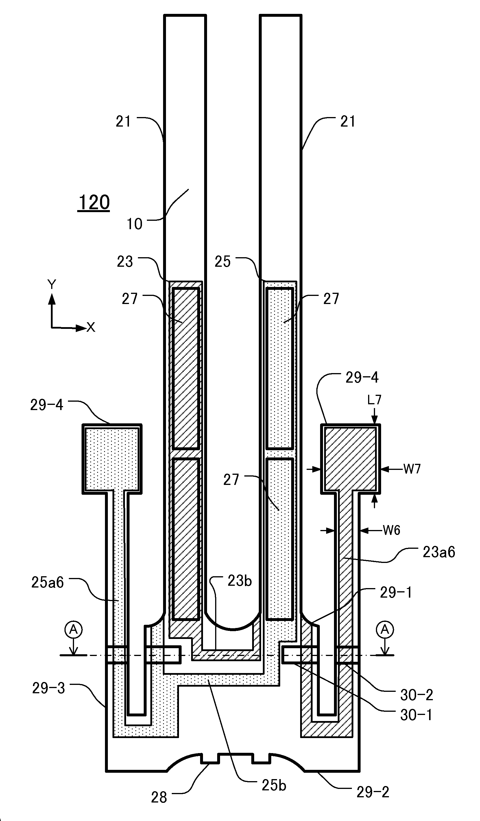
[0068]Current demand is for very small tuning-fork type crystal vibrating devices. As these devices are configured with increasingly complex shapes, they are more likely to be damaged during manufacture. However, their precision is increased. By employing the manufacturing processes of the first and second embodiments, smaller tuning-fork type crystal vibrating devices can be formed more precisely and with less collateral damage.
[0069]FIG. 6A shows, by way of example, a tuning-fork type crystal vibrating device 120 having small size and a complex shape. (Certain reference numbers in FIG. 6A are the same as corresponding reference numbers used in FIG. 1A for similar elements.) The crystal vibrating device 120 can be formed with a smaller base 29 than the base on the device 20, and the length of the device 120 in the Y-direction can be shorter than the length of the device 20.
[0070]The crystal vibrating device 120 i...
PUM
| Property | Measurement | Unit |
|---|---|---|
| Thickness | aaaaa | aaaaa |
Abstract
Description
Claims
Application Information
 - R&D
- Intellectual Property
- Life Sciences
- Materials
- Tech Scout
- Unparalleled Data Quality
- Higher Quality Content
- 60% Fewer Hallucinations
Browse by: Latest US Patents, China's latest patents, Technical Efficacy Thesaurus, Application Domain, Technology Topic, Popular Technical Reports.
© 2025 PatSnap. All rights reserved.Legal|Privacy policy|Modern Slavery Act Transparency Statement|Sitemap|About US| Contact US: help@patsnap.com