Light emitting device

a light emitting device and light technology, applied in the direction of semiconductor/solid-state device manufacturing, semiconductor devices, electrical devices, etc., can solve the problems of lowering efficiency, light extraction efficiency that is only about 1.2-1.5 times that achieved, and the geometrical adjustment of the light extraction device's geometric dimensions for enhancing light extraction efficiency has not been known. , to achieve the effect of enhancing light extraction efficiency

Inactive Publication Date: 2009-03-26
SHOWA DENKO KK
View PDF11 Cites 39 Cited by
  • Summary
  • Abstract
  • Description
  • Claims
  • Application Information

AI Technical Summary

Benefits of technology

[0007]It is an object of the present invention to provide a light emitting device with excellent light extraction efficiency due to reduced self-absorption of light from the light emitting element.
[0008]According to the present invention, the spacing between the top and bottom surfaces of the cap is a specific length and a specified distance is provided between the light emitting element and the cap top surface (light extraction surface), while the cap shape is also modified to reduce self-absorption of light from the light emitting element and enhance the light extraction efficiency. Specifically, the invention provides the following.
[0021]According to the light emitting device of the invention, the spacing (height) between the top and bottom surfaces of the cap is set to be greater than the longest diagonal or the diameter of the light emitting element, whereby light emitted from the light emitting element is efficiently extracted from the sealed structure and self-absorption of light from the light emitting element is prevented to enhance the light extraction efficiency. Furthermore, by forming a suitable angle between the sides and top surface of the cap, it is possible to further enhance the light extraction efficiency.
[0022]In addition, the light emitting element is sealed in a manner that also enhances light extraction efficiency and the light emitting element is situated at the focus of a parabolic reflector, in order to provide a light emitting device with high front brightness.

Problems solved by technology

In such light emitting devices, a material having a refractive index intermediate between the light emitting element and air is employed as the sealing material in order to reduce total reflection in the light emitting element, but self-absorption of light from the light emitting element also occurs, along the beam trajectory indicated by A in FIG. 1, thereby lowering the efficiency and specifically resulting in light extraction efficiency that is only about 1.2-1.5 times that achieved without sealing.
However, adjustment of the geometric dimensions in a light emitting element-mounted light emitting device for enhancement of light extraction efficiency has not been known.

Method used


Image

  • Light emitting device
  • Light emitting device
  • Light emitting device

Examples


example 1

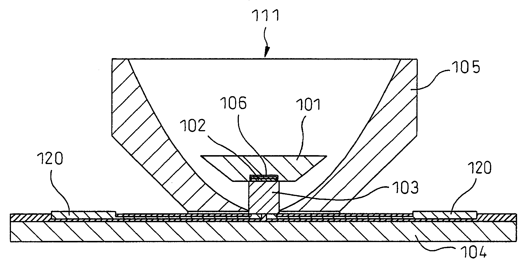
[0073]A first example of a light emitting device according to the invention will now be described with reference to the accompanying drawings. FIG. 14 is a cross-sectional view of the light emitting device fabricated in this example, and FIG. 15 is a plan view of the same. The light emitting device 111 is composed of a radiating board 104, reflector 105, submount 103, semiconductor light emitting element 102 and cap 101. The numeral 106 represents a sealing compound. Also, the numeral 120 represents an external power source connection electrode and the numeral 121 represents a heat sink fitting section.

[0074]The semiconductor light emitting element 102 used is the GaN-based compound semiconductor blue light emitting element described below, having a square shape with 1 mm×1 mm sides and a thickness of about 90μ.

[0075]On a sapphire substrate was stacked a ground layer composed of undoped GaN with a thickness of 8 μm, a Ge-doped n-type GaN contact layer with a thickness of 2 μm, an n-...

example 2

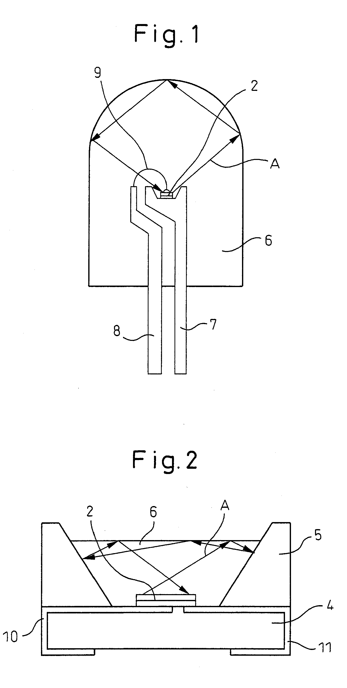
[0092]FIG. 17 shows a cross-sectional view of a light emitting device fabricated for this example. A light emitting device was fabricated in the same manner as Example 1, except that the shape of the cap 101 was a clipped conical shape with a top surface radius of 0.8 mm, a bottom surface radius of 1.6 mm and a height of 1.5 mm, so that the top and bottom surface area ratio was 1:4 and the top and bottom surface spacing was a distance greater than the longest diagonal of the light emitting element. When the obtained light emitting device was subjected to a current test in the same manner as Example 1, the light extraction was approximately 1.87 times that of a bare chip.

[0093]When the front brightnesses of the light emitting device of Example 1 and the light emitting device of Example 2 were compared, that of the light emitting device of Example 2 was 0.2 compared to 1 as the light emitting device of Example 1.


PUM


Abstract

A light emitting device includes a board, a semiconductor light emitting element formed on the board optionally via a submount, a cap sealing the semiconductor light emitting element and a reflector provided surrounding the cap. The cap has top and bottom surfaces that are parallel to the top surface of the semiconductor light emitting element, and the spacing between the top and bottom surfaces is 1-3 times the longest diagonal or the diameter of the semiconductor light emitting element. Also disclosed is a process for producing the device.

Description

CROSS REFERENCE TO RELATED APPLICATION[0001]This application is an application filed under 35 U.S.C. §111(a) claiming benefit, pursuant to 35 U.S.C. §119(e)(1), of the filing date of the Provisional Application No. 60 / 775,798 filed on Feb. 23, 2006, pursuant to 35 U.S.C. §111(b).TECHNICAL FIELD[0002]The present invention relates to a light emitting device and, particularly, to a light emitting device with enhanced light extraction efficiency. The efficiency is improved by reducing the self-absorption of light from a light emitting element due to total reflection of light at the light extraction surface formed by a lens or sealing material covering the light emitting element.BACKGROUND ART[0003]Examples of known light emitting devices employing light emitting elements include a light emitting device such as that shown in FIG. 1 which has a lamp-type light emitting diode mounted on a lead frame and sealed in resin, and a light emitting device such as shown in FIG. 2 which has a board,...

Claims


Application Information

Patent Timeline
Patent Type & Authority Applications(United States)
IPC IPC(8): H01L33/00H01L21/00H01L33/06H01L33/32H01L33/54H01L33/60H01L33/62
CPCH01L33/54H01L33/60H01L2224/48091H01L2224/48247H01L2224/73265H01L2924/00014H01L2924/181H01L2924/00012
Inventor HOSHINA, TAKAHARU
Owner SHOWA DENKO KK
Why Eureka
Try Eureka