Circuit board, electronic device and method for manufacturing the same

a technology of electronic devices and circuit boards, applied in the direction of resistive material coatings, solid-state devices, metallic pattern materials, etc., can solve the problems of circuit boards to a high temperature, oxidizing the surface of circuit patterns, and increasing the signal delay between lsis, so as to avoid the formation of voids due to flux gas and eliminate voids

Inactive Publication Date: 2009-04-02
NAPRA
View PDF3 Cites 31 Cited by
  • Summary
  • Abstract
  • Description
  • Claims
  • Application Information

AI Technical Summary

Benefits of technology

[0024]The oxide film, which has been produced on the surface of the circuit pattern at the bottom of the through-hole before filling the molten metal material of the through electrode, can be reduced by catalysis of the noble metal particles. Thus, since the reduction does not need any flux, formation of voids due to a flux gas can be avoided.
[0025]As another aspect of the present invention, the through electrode may contain bismuth (Bi), gallium (Ga) and antimony (Sb). In the case of containing bismuth (Bi), gallium (Ga) and antimony (Sb), it is possible to eliminate voids from the resulting through electrode by using their cubical expansion properties.

Problems solved by technology

However, this method increases the mounting area with the number of LSIs, so that the signal delay between LSIs increases because of an increase in wiring length.
Such thin-film formation techniques expose the circuit board to a high temperature.
This results in oxidizing the surface of the circuit pattern at the inner bottom surface of the through-holes.
Oxidation of the surface of the circuit pattern to be connected to the through electrodes deteriorates the connection between the circuit pattern and the through electrodes, thereby causing serious problems that cannot be overlooked in electronic devices of this type, such as insufficient properties and a decrease in yield.
However, the above reduction technique using a flux causes the following serious problem.
If a flux gas is generated in such through-holes, the escape of gas inevitably becomes difficult, producing voids due to the flux gas around the through electrodes, which leads to a decrease in cross-sectional area of the through electrodes, an increase in electrical resistance, poor connection to the circuit pattern, and an increase in bond resistance.

Method used


Image

  • Circuit board, electronic device and method for manufacturing the same
  • Circuit board, electronic device and method for manufacturing the same
  • Circuit board, electronic device and method for manufacturing the same

Examples


Embodiment Construction
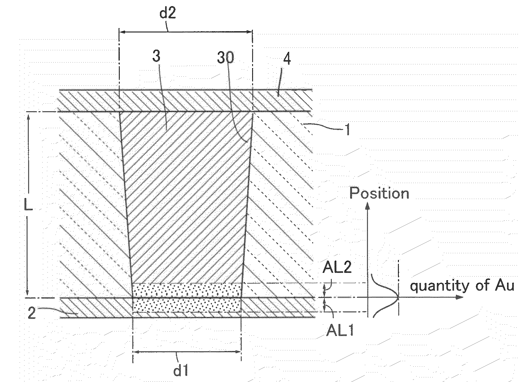
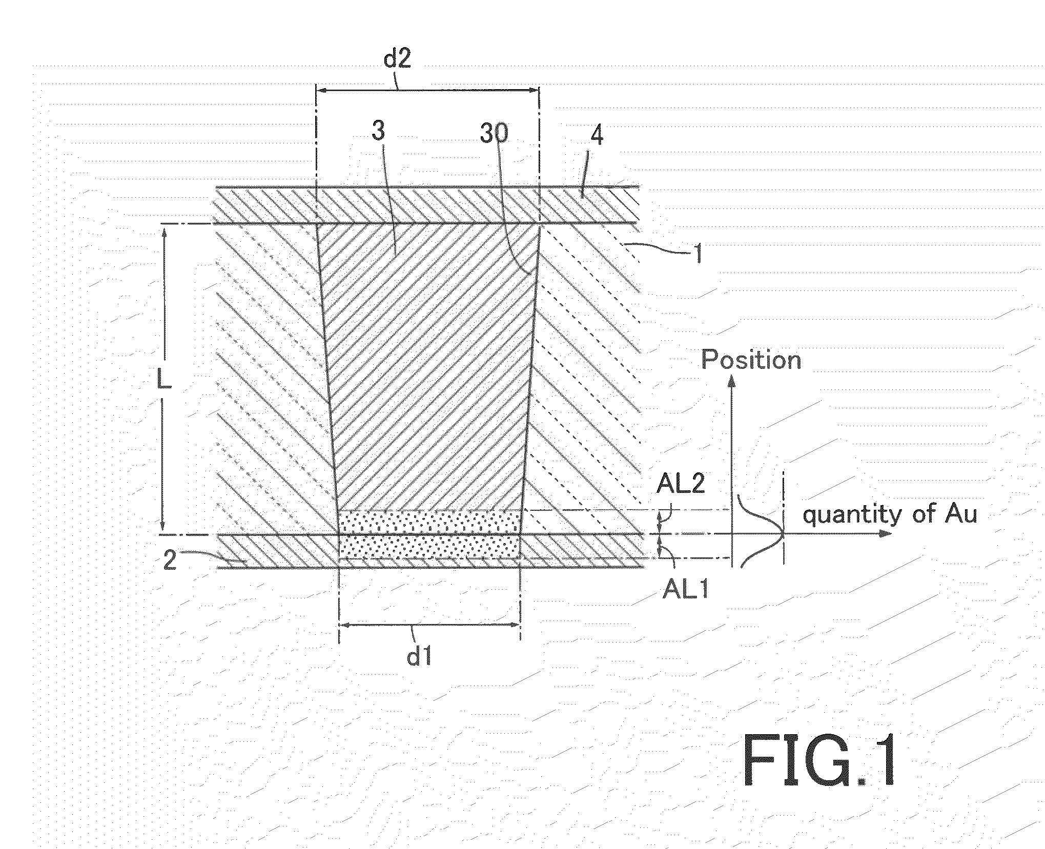
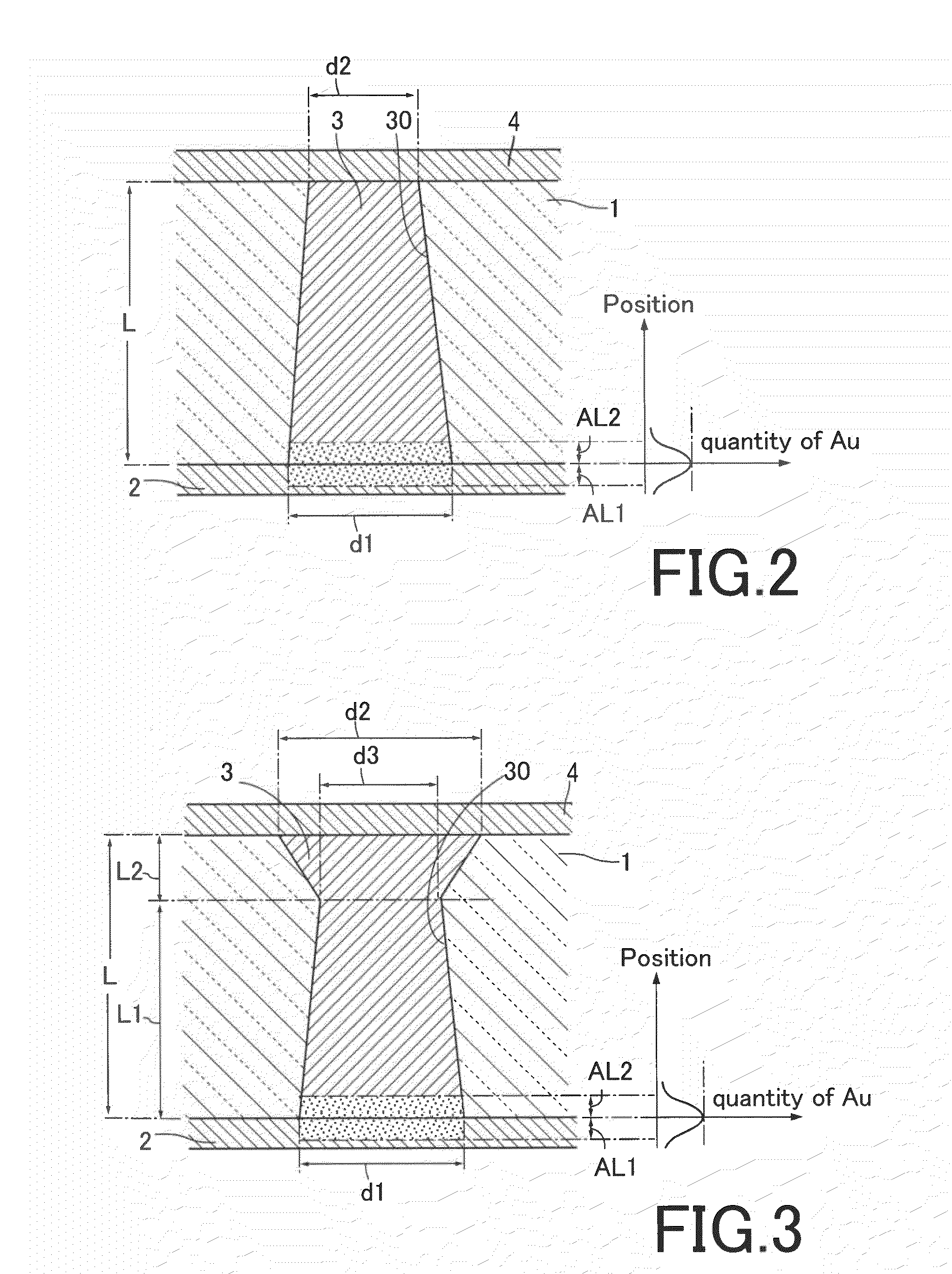
(Circuit Board)

[0050]Referring to FIG. 1, there is shown a circuit board having a simple configuration, but in practice, it has a more complicated configuration so as to satisfy functional and structural requirements depending on the type of the circuit board. The illustrated circuit board has a three-dimensional circuit configuration composed of a substrate 1, a circuit pattern 2 and a through electrode 3. The substrate 1 may be various types of semiconductor substrates, a dielectric substrate, an insulating substrate or a magnetic substrate. In the illustrate embodiment, the substrate 1 is a semiconductor substrate, e.g., a silicon wafer. In the case of a semiconductor substrate, an insulating film is disposed on both sides and an interface between the through electrode 3 and the substrate 1. The insulating film may be a film of a metal oxide such as SiO2 and Al2O3 and can be formed with a required thickness (depth) at a required location through a known chemical treatment.

[0051]T...


PUM

PropertyMeasurementUnit
grain sizeaaaaaaaaaa
diameter d1aaaaaaaaaa

Abstract

A circuit board includes a substrate, a circuit pattern and a through electrode. The circuit pattern is disposed on one side of the substrate in a thickness direction thereof. The through electrode is filled in a through-hole formed in the substrate with one end connected to the circuit pattern. The circuit pattern and the through electrode each have an area containing a noble metal component (e.g., Au component) and are connected to each other therethrough.

Description

BACKGROUND OF THE INVENTION[0001]1. Field of the Invention[0002]The present invention relates to a circuit board, an electronic device and a method for manufacturing the same.[0003]2. Description of the Related Art[0004]Examples of electronic device include various scales of integrated circuits and various types of semiconductor devices and chips thereof.[0005]As means for realizing a three-dimensional circuit configuration in electronic devices of this type, there has been adopted a method that LSIs are disposed on a circuit board with multilayered wiring therebetween. However, this method increases the mounting area with the number of LSIs, so that the signal delay between LSIs increases because of an increase in wiring length.[0006]Accordingly, there has been proposed a technology of using a circuit board with a circuit pattern disposed on one side and through electrodes passing therethrough in a thickness direction and connected to the circuit pattern.[0007]As one example of suc...

Claims


Application Information

Patent Timeline
Patent Type & Authority Applications(United States)
IPC IPC(8): B05D5/12H05K1/00H05K1/09
CPCH01L21/76898Y10T29/49155H05K3/4038H05K3/4061H05K3/4614H05K2201/0215H05K2201/0218H05K2201/0305H05K2201/0394H05K2201/083H05K2203/0285H05K2203/104H05K2203/128H01L23/481Y10T29/49156H01L2924/0002H01L2924/00012H01L2924/00
Inventor SEKINE, SHIGENOBUSEKINE, YURINAKUWANA, YOSHIHARU
Owner NAPRA
Why Eureka
Try Eureka