Method for preventing doped boron in a dielectric layer from diffusing into a substrate

a dielectric layer and substrate technology, applied in the direction of semiconductor devices, electrical equipment, basic electric elements, etc., can solve the problems of difficult for bpsg to fill the space between the gates, void formation, and serious effect of boron diffusion, so as to reduce the thickness of the barrier layer, reduce the aspect ratio of the memory array area, and avoid the formation of voids in the memory array area

Inactive Publication Date: 2007-04-26
PROMOS TECH INC
View PDF3 Cites 0 Cited by
  • Summary
  • Abstract
  • Description
  • Claims
  • Application Information

AI Technical Summary

Benefits of technology

[0015] Accordingly, the method of the present invention has advantages especially when a substrate comprises both a memory array area and a periphery circuit area. In the present invention, the diffusion of boron into the substrate can be avoided in the periphery circuit area since an undoped oxide barrier is formed in the periphery circuit area. Furthermore, the aspect ratio in the memory array area can be reduced and the formation of voids in the memory array area can be avoided since the thickness of the barrier layer is reduced.

Problems solved by technology

The diffusion of the boron has a serious effect, particularly on PMOS.
Therefore, it is not easy for BPSG to fill the space between the gates in the memory array area, and voids are formed between the gates.
Consequently, the thickness of the silicon oxynitride layer or the silicon nitride layer becomes so thin that it is no longer sufficient to prevent boron from diffusing into the substrate.

Method used


Image

  • Method for preventing doped boron in a dielectric layer from diffusing into a substrate
  • Method for preventing doped boron in a dielectric layer from diffusing into a substrate

Examples


Embodiment Construction

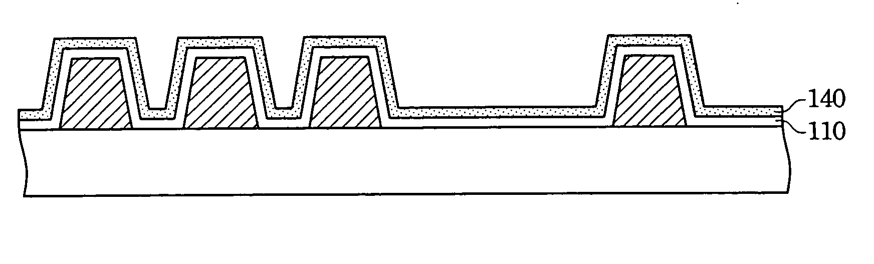
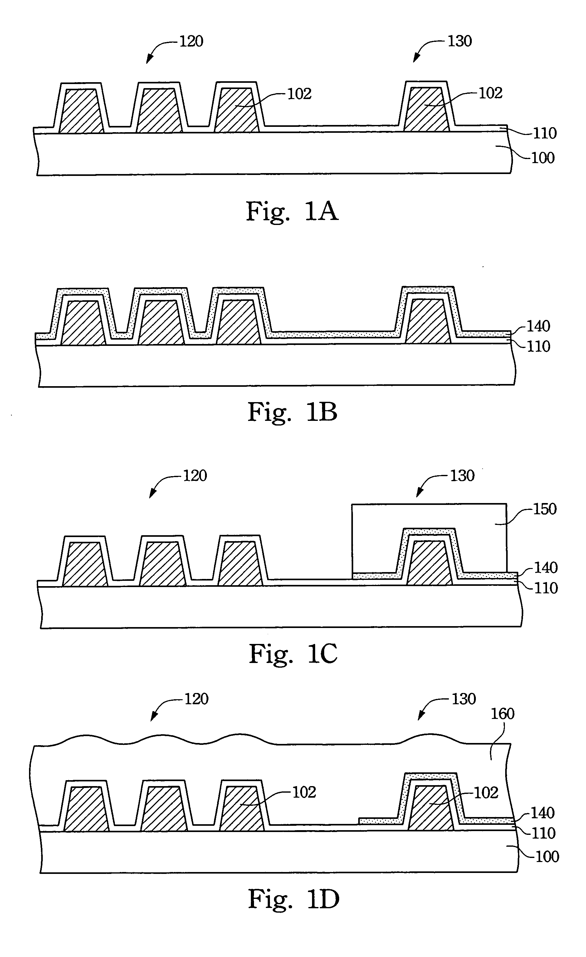
[0018]FIG. 1A to FIG. 1D are cross-sectional views showing a flowchart of depositing a boron-containing silicate glass onto a silicon substrate according to a preferred embodiment of the present invention.

[0019] In FIG. 1A, at least one gate 102 is formed in each of a memory array area 120 and in a periphery circuit area 130 of a substrate 100, respectively. A barrier layer 110 is formed in the memory array area 120 and the periphery circuit area 130. Preferably, the barrier layer 110 is a silicon nitride layer. The pattern density in the memory array area 120 is higher than that in the periphery circuit area 130, and is preferably higher than 1. The memory array area 120 is usually an area with higher pattern density and is not usually affected by boron diffusion because only NMOS is used in this area as memory cells. Conversely, the periphery circuit area 130 is usually an area with lower pattern density and where the diffusion of boron into the substrate must be avoided because ...


PUM


Abstract

The present invention provides a method for preventing doped boron in a dielectric layer from diffusing into a substrate. First, at least one gate is formed on a periphery circuit area and a memory array area of a substrate, respectively, wherein the pattern density in the memory array area is higher than that in the periphery circuit area. Then, a barrier layer is formed on the memory array area and the periphery circuit area, and an undoped oxide barrier is formed on the periphery circuit area. Finally, a silicate glass containing boron is deposited on the memory array area and the periphery circuit area.

Description

BACKGROUND [0001] 1. Field of Invention [0002] The present invention relates to a method for producing a semiconductor device. More particularly, the present invention relates to a method for preventing doped boron in a dielectric layer from diffusing into a substrate and for avoiding voids forming in the high-pattern-density area of the substrate. [0003] 2. Description of Related Art [0004] Generally, a memory device comprises a periphery circuit area and a memory array area. The periphery circuit area has lower pattern density and usually comprises PMOS and NMOS. On the contrary, the memory array area has higher pattern density and usually uses only NMOS as a memory cell to constitute a memory device. The term “pattern density” means the ratio of gate area to non-gate area. (line to space) [0005] Borophosphosilicate glass (BPSG) is a silicon oxide doped with boron and phosphorus and is a material commonly used for an inter-layer-dielectric layer in a semiconductor process. An undo...

Claims


Application Information

Patent Timeline
Patent Type & Authority Applications(United States)
IPC IPC(8): H01L21/8234H01L21/8238
CPCH01L21/823456H01L27/105H01L27/1052H10B99/00
Inventor HSIAO, CHIA-SHUNTUNG, MING-SHENGCHEN, HONG-MINGHUANG, CHING-HSIEN
Owner PROMOS TECH INC
Why Eureka
Try Eureka