Production method of shallow channel isolation region

A technique for shallow trench isolation and a manufacturing method, which is applied in the field of manufacturing shallow trench isolation regions, can solve problems such as etching residues, affecting isolation effects, and polysilicon residues, so as to reduce the formation of missing corners and avoid slow deposition rates. average effect

Active Publication Date: 2013-04-17
SEMICON MFG INT (SHANGHAI) CORP
View PDF3 Cites 0 Cited by
  • Summary
  • Abstract
  • Description
  • Claims
  • Application Information

AI Technical Summary

Problems solved by technology

However, STI also has many technical problems in the process, such as the shape control of STI, the rounding of the top corner of STI, the adaptation stress between the silicon dioxide inside the STI and the external silicon, and the defect of the top edge of the shallow trench isolation region. Corner problem (STI Divot), etc.
in, figure 1 It is a schematic diagram of the notch problem at the top edge of the shallow trench isolation region in the prior art, refer to figure 1 In the step of removing the mask layer 102', the mask layer 102' is wet-cleaned. During the wet-cleaning process, the top edge of the oxide isolation layer 103' will be corroded, resulting in more or even larger The problem of notch 10 on the top edge of the shallow trench isolation region, the problem caused by the notch 10 on the top edge of the shallow trench isolation region will be directly related to the leakage problem at the edge of the STI, which will affect the characteristics of the device, because the top edge of the shallow trench isolation region The formation of the notch 10 at the edge leads to the formation of an inversion layer on the side of the active region when the gate is filled, resulting in a parasitic current path, which in turn affects the characteristics of the device, and the notch at the top edge of the shallow trench isolation region that is too deep 10 will increase the difficulty of etching the polysilicon gate and silicon nitride sidewall, and may cause etching residues. Therefore, controlling the size and depth of the notch 10 on the top edge of the shallow trench isolation region has attracted more and more attention.
However, this method also has problems, that is, after the mask layer 102' is etched back, the angle at the step of the channel is generally about 270°, and when the oxide isolation layer 103' is deposited, the angle at the step is generally Because the angle is larger and the deposition speed is faster than other places, the channel will be sealed in advance, resulting in incomplete filling of the void 30 (void) inside the channel, which will affect the isolation effect, and will also cause subsequent polysilicon growth. The polysilicon remains in the cavity 30, which affects the leakage of components and parts, and in severe cases, a short circuit will be formed

Method used


Image

  • Production method of shallow channel isolation region
  • Production method of shallow channel isolation region
  • Production method of shallow channel isolation region

Examples


Embodiment Construction

[0035] In order to make the content of the present invention clearer and easier to understand, the content of the present invention will be further described below in conjunction with the accompanying drawings. Of course, the present invention is not limited to this specific embodiment, what is the technology in this field? Common substitutions known to persons are also covered within the protection scope of the present invention.

[0036] Secondly, the present invention is described in detail by means of schematic diagrams. When describing the examples of the present invention in detail, for the convenience of explanation, the schematic diagrams are not partially enlarged according to the general scale, which should not be used as a limitation of the present invention.
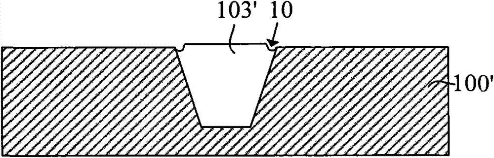
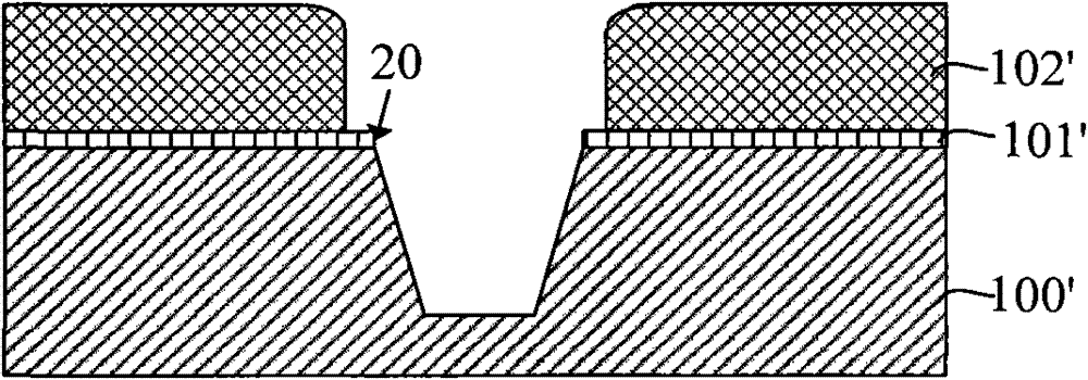
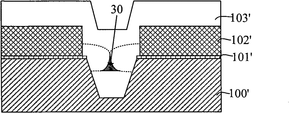
[0037] The core idea of ​​the present invention is: after the step of forming the oxide isolation layer, the mask layer is etched back, and an oxide layer is formed between the oxide isolation layer and the m...


PUM


Abstract

The invention relates to a production method of a shallow channel isolation region, which comprises the following steps that: a semiconductor underlay is provided, a mask layer is formed on the semiconductor underlay, the semiconductor underlay is etched to form a channel, an oxidized isolation layer is formed to fill the channel, etching-back processing on the mask layer is undertaken after the oxidized isolation layer is smoothened, a gap is formed between the oxidized isolation layer and the mask layer, and an oxidized layer is formed to fill the gap. By forming the gap between the mask layer and the oxidized isolation layer and by filling the gap with the oxidized layer, not only can the hollow formation problem inside the oxidized isolation layer be avoided, but also the corrosion isdifficult to happen in the subsequent wet-method washing process, and the broken corner formation problem on the top edge of the shallow channel isolation region can be effectively reduced.

Description

technical field [0001] The invention relates to the field of semiconductor manufacturing, in particular to a method for manufacturing a shallow trench isolation region. Background technique [0002] In recent years, with the development of semiconductor integrated circuit manufacturing technology, the number of components contained in the chip has been increasing, and the size of the components has been continuously reduced due to the improvement of integration. The line width used in the production line has entered the sub-micron level. scope. However, no matter how the device size is reduced, there must still be proper insulation or isolation between the various devices in the chip in order to obtain good device properties. The technology in this area is generally called Device Isolation Technology (Device Isolation Technology), and its main purpose is to form spacers between the components, and to ensure good isolation effect, minimize the area of ​​the spacers to free u...

Claims


Application Information

Patent Timeline
Patent Type & Authority Patents(China)
IPC IPC(8): H01L21/762H01L21/316
Inventor 宁振佳
Owner SEMICON MFG INT (SHANGHAI) CORP
Why Eureka
Try Eureka