Semiconductor device and method for manufacturing the same

a semiconductor device and semiconductor technology, applied in the field of semiconductor devices, can solve the problems of reduced yield compared with the tag with the on-chip, insufficient resistance to external force, easy cutting of the connection between the integrated circuit and the antenna, etc., and achieve the effect of preventing the damage of a semiconductor device, high tensile modulus of elasticity, and high young's modulus

Inactive Publication Date: 2009-04-02
SEMICON ENERGY LAB CO LTD
View PDF55 Cites 43 Cited by
  • Summary
  • Abstract
  • Description
  • Claims
  • Application Information

AI Technical Summary

Benefits of technology

[0014]As the fiber body, a woven fabric or a nonwoven fabric using a high-strength fiber of an organic compound or an inorganic compound can be used. The high-strength fiber is specifically a fiber with a high tensile modulus of elasticity or a high Young's modulus. By using the high-strength fiber as the fiber body, even when pressing force is locally applied to a semiconductor device, the pressure is distributed to the whole fiber body, and a part of the semiconductor device being stretched can be prevented. That is, destruction of

Problems solved by technology

However, in the case of an RF tag using a flexible substrate, connection between an integrated circuit and an antenna is easily cut when external force is applied to the substrate, and reliability in terms of resistance to external force is not quite sufficient compared with the tag with the on-chip antenna.
Moreover, initial defects at a connection portion of the integrated circuit and the antenna cause reduction in yield compared with the tag with the on-chip antenna.
Accordingly, a problem occurs where the above-desc

Method used


Image

  • Semiconductor device and method for manufacturing the same
  • Semiconductor device and method for manufacturing the same
  • Semiconductor device and method for manufacturing the same

Examples


embodiment mode 1

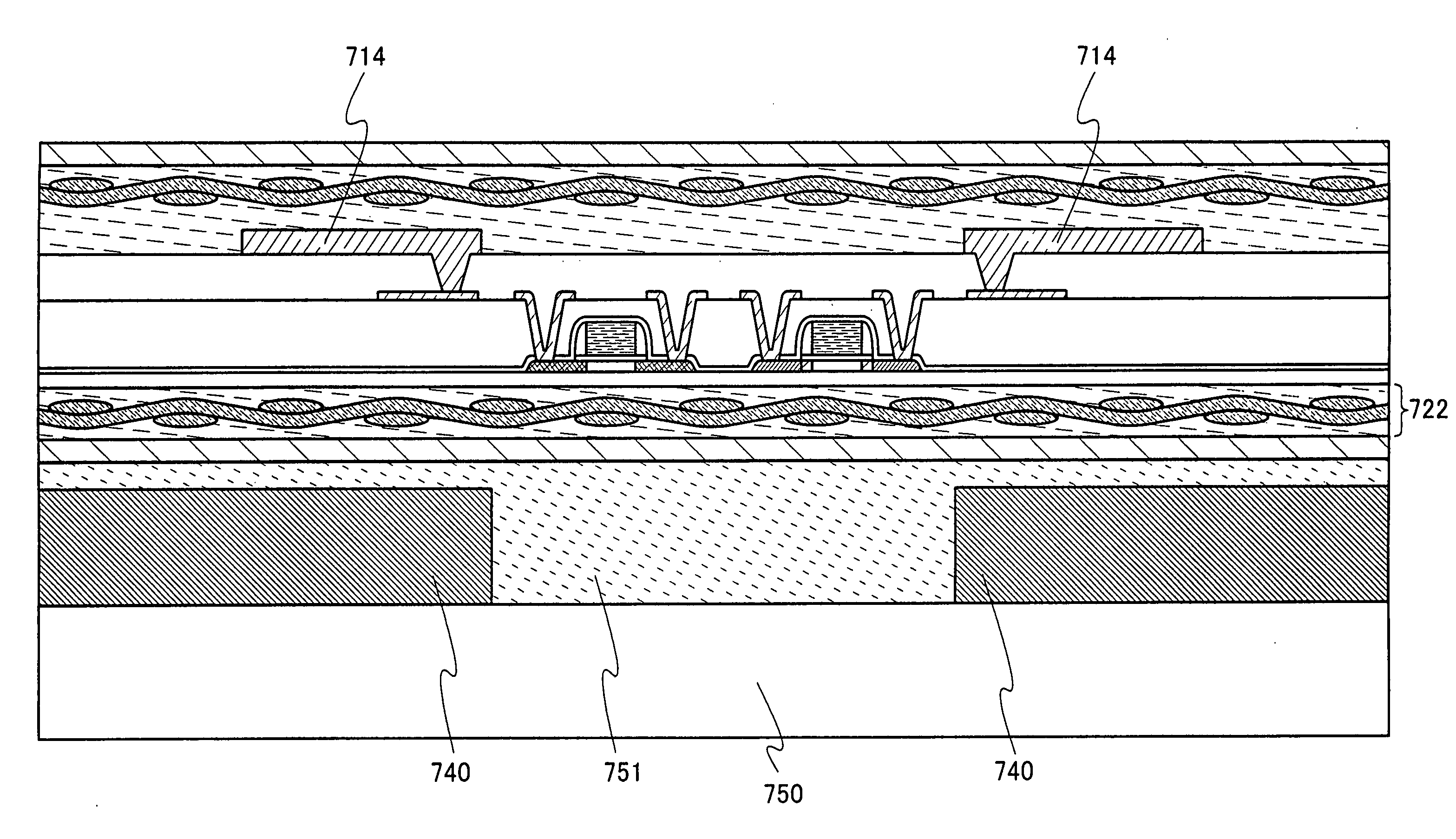
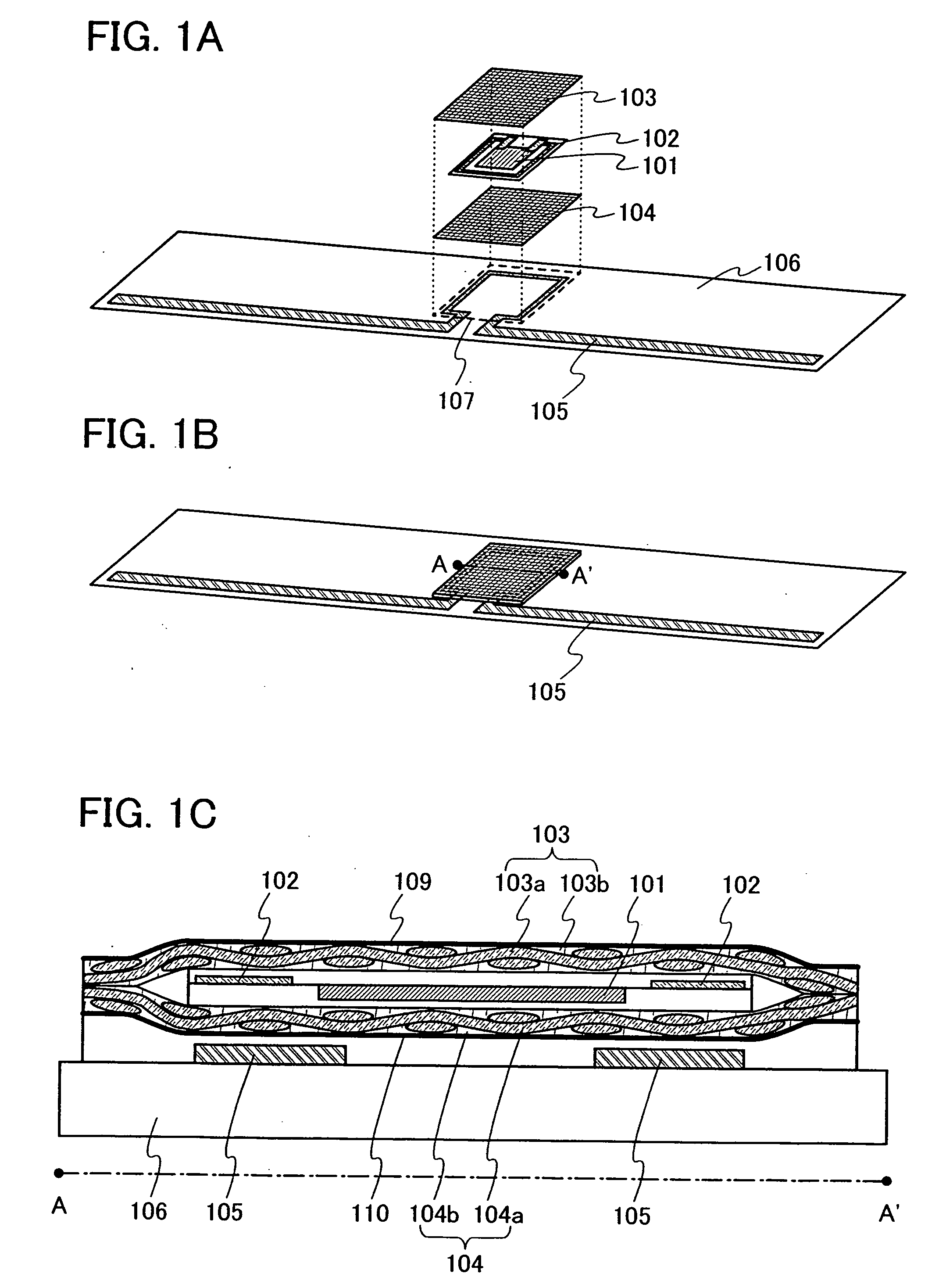
[0037]FIG. 1A is a perspective view illustrating a stacked-layer structure of a semiconductor device of the present invention. The semiconductor device of the present invention includes an integrated circuit 101 and an on-chip antenna 102 connected to the integrated circuit 101. The integrated circuit 101 and the on-chip antenna 102 are formed in an integrated manner. That is, the on-chip antenna 102 is directly formed on the integrated circuit 101 and is formed so as to be connected to the integrated circuit 101. The integrated circuit 101 and the on-chip antenna 102 are provided between structure bodies 103 and 104 formed by impregnating a fiber body with a resin. Moreover, the semiconductor device of the present invention includes a booster antenna 105. The structure body 104 is interposed between the on-chip antenna 102 and the booster antenna 105. Note that FIG. 1A illustrates an example in which the booster antenna 105 is formed over a supporting substrate 106.

[0038]FIG. 4A is...

embodiment mode 2

[0076]The inventors examined an operation rate of the semiconductor device of the present invention when voltage is applied using an ESD tester.

[0077]In the test for the operation rate of the semiconductor devices, all samples have a structure in which an on-chip antenna and an integrated circuit are interposed between a pair of structure bodies each including a single-layer fiber body. The area of the semiconductor device is 0.5 mm×12.0 mm. The fiber body is plain-woven using the warp yarn and the weft yarn. A sample A is a sample in which an antistatic film is not formed. A sample B is a sample in which an antistatic film is formed on the side of each structure body, which does not face the on-chip antenna and the integrated circuit as in FIG. 1C, and a cationic surfactant (product name: Staticide (registered trademark), manufactured by ACL Staticide Inc.) is used for the antistatic film. A sample C is a sample in which an antistatic film is formed on the side of each structure bo...

embodiment mode 3

[0080]The inventors examined the amount of charging in the semiconductor device of the present invention when friction treatment is performed.

[0081]In the test for the amount of charging, all samples have a structure in which an on-chip antenna and an integrated circuit are interposed between a pair of structure bodies each including a single-layer fiber body. The fiber body included in the structure body is plain-woven using the warp yarn and the weft yarn. A sample A is a sample in which an antistatic film is not formed. A sample B is a sample in which an antistatic film is formed on the side of each structure body, which does not face the on-chip antenna and the integrated circuit as in FIG. 1C, and siloxane-based oligomer (product name: COLCOAT, manufactured by COLCOAT CO., Ltd.) is used for the antistatic film. A sample C is a sample in which an antistatic film is formed on the side of each structure body, which faces the on-chip antenna and the integrated circuit as in FIG. 3A...


PUM


Abstract

A semiconductor device capable of wireless communication, which has high reliability in terms of resistance to external force, in particular, pressing force and can prevent electrostatic discharge in an integrated circuit without preventing reception of an electric wave. The semiconductor device includes an on-chip antenna connected to the integrated circuit and a booster antenna which transmits a signal or power included in a received electric wave to the on-chip antenna without contact. In the semiconductor device, the integrated circuit and the on-chip antenna are interposed between a pair of structure bodies formed by impregnating a fiber body with a resin. One of the structure bodies is provided between the on-chip antenna and the booster antenna. A conductive film having a surface resistance value of approximately 106 to 1014 Ω/cm2 is formed on at least one surface of each structure body.

Description

BACKGROUND OF THE INVENTION[0001]1. Field of the Invention[0002]The present invention relates to a semiconductor device which can perform wireless communication and a manufacturing method thereof.[0003]2. Description of the Related Art[0004]A technology by which an individual object is identified by wirelessly transmitting and receiving signals (RFID: radio frequency identification) has been put into practical use in a variety of fields, and further expansion of the market for such a technology as a new mode of information communication is expected. An RF tag is also referred to as an ID chip, a wireless tag, or an IC tag, and typically includes an antenna and an integrated circuit (an IC chip) formed using a semiconductor substrate. In RFID, signals are generally transmitted and received wirelessly between an interrogator, which is also referred to as a reader or a reader / writer, and an RF tag. RF tags often take the form of cards, or chips, which are smaller than cards. However, t...

Claims


Application Information

Patent Timeline
IPC IPC(8): H01L21/58H01L23/12
CPCH01L23/295H01L23/3157H01L2924/09701H01L2924/12044H01L2924/19041H01L2924/3011G06K19/07794H01L2924/0002H01L2924/3025G06K19/07735G06K19/07722H01L2924/00H01Q1/24
Inventor YAMAZAKI, SHUNPEIKOYAMA, JUNKATO, KIYOSHIKOEN, TAKAAKIYAKUBO, YUTOYANAGISAWA, MAKOTOOHTANI, HISASHISUGIYAMA, EIJIHORIKOSHI, NOZOMI
Owner SEMICON ENERGY LAB CO LTD
Why Eureka
Try Eureka