Method and system for split voltage domain receiver circuits

a receiver circuit and split voltage technology, applied in the field of integrated circuit power control, can solve problems such as excessive leakage, degrade performance, and drive gate voltages lower

Active Publication Date: 2009-04-02
CISCO TECH INC
View PDF9 Cites 11 Cited by
  • Summary
  • Abstract
  • Description
  • Claims
  • Application Information

AI Technical Summary

Benefits of technology

[0016]FIG. 1D is a block diagram of an exemplary n-type field effect transistor circuit, in accordance with an embodiment of the invention.
[0017]FIG. 1E is a block diagram of an exemplary p-type field effect transistor circuit, in accordance with an embodiment of the invention.

Problems solved by technology

Furthermore, as device sizes continue to shrink for higher speed and lower power consumption, a high voltage may degrade performance and cause excessive leakage.
With thinner gate oxides, gate leakage current may become significant using historical bias voltages, thus driving gate voltages lower.
However, if a transmitter / receiver may be integrated in the same device, a higher bias voltage may also be required.
However, there may be noise in the bias voltage, which may be mitigated by capacitive filters.

Method used


Image

  • Method and system for split voltage domain receiver circuits
  • Method and system for split voltage domain receiver circuits
  • Method and system for split voltage domain receiver circuits

Examples


Embodiment Construction

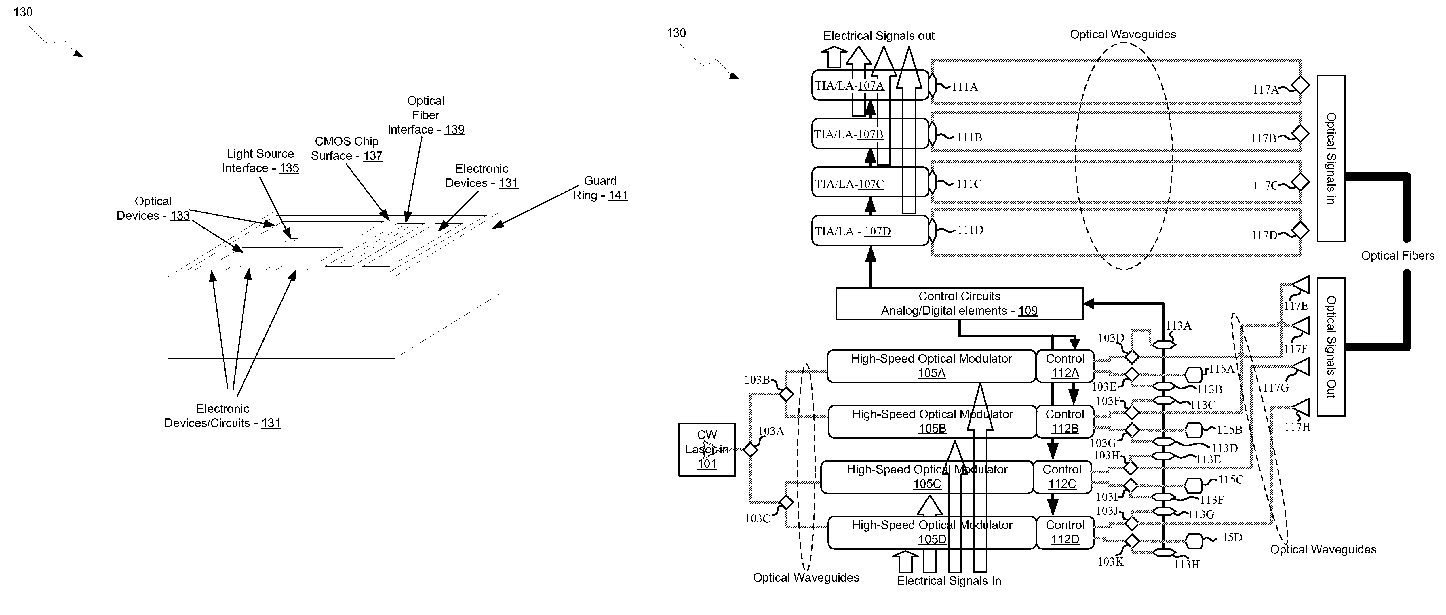
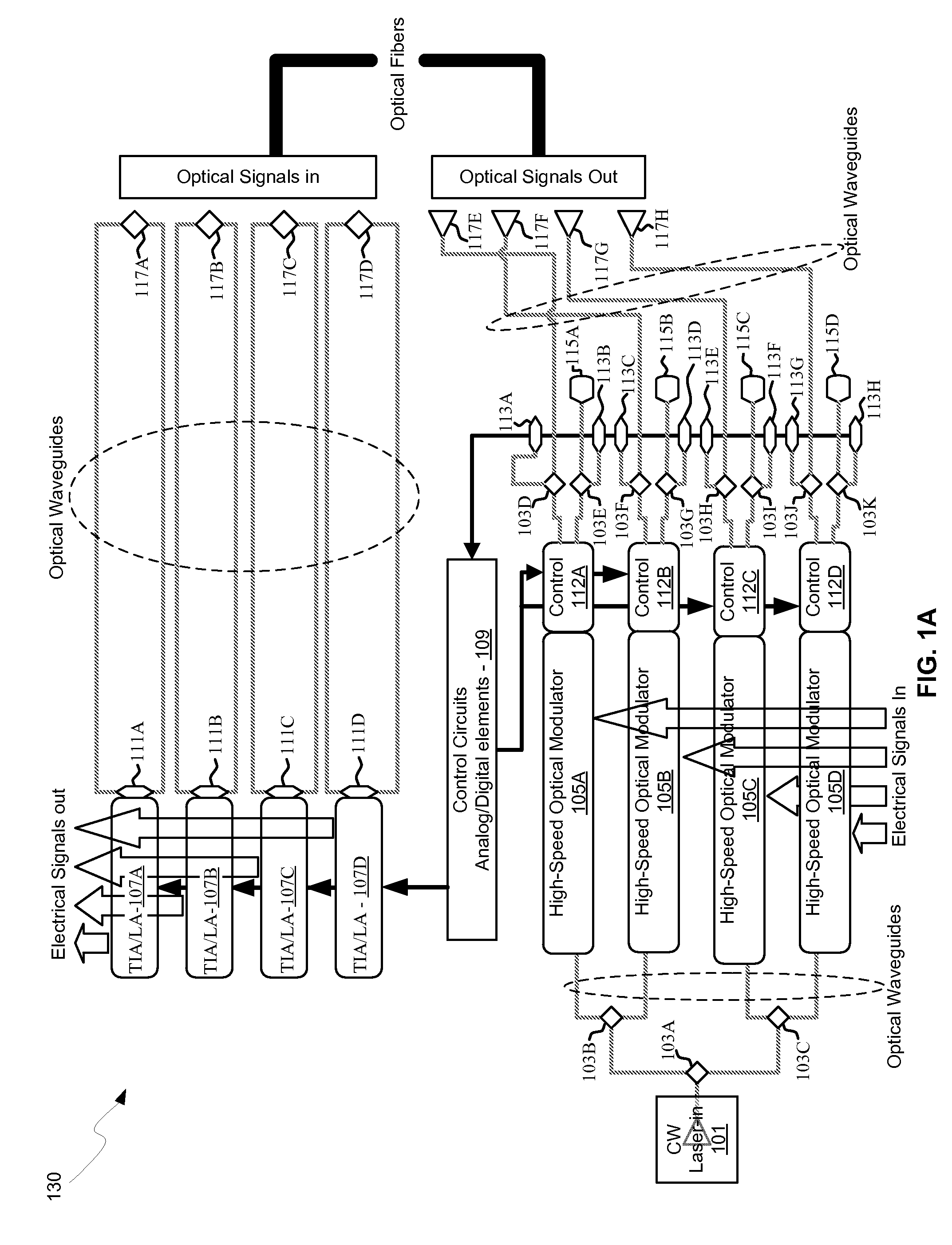
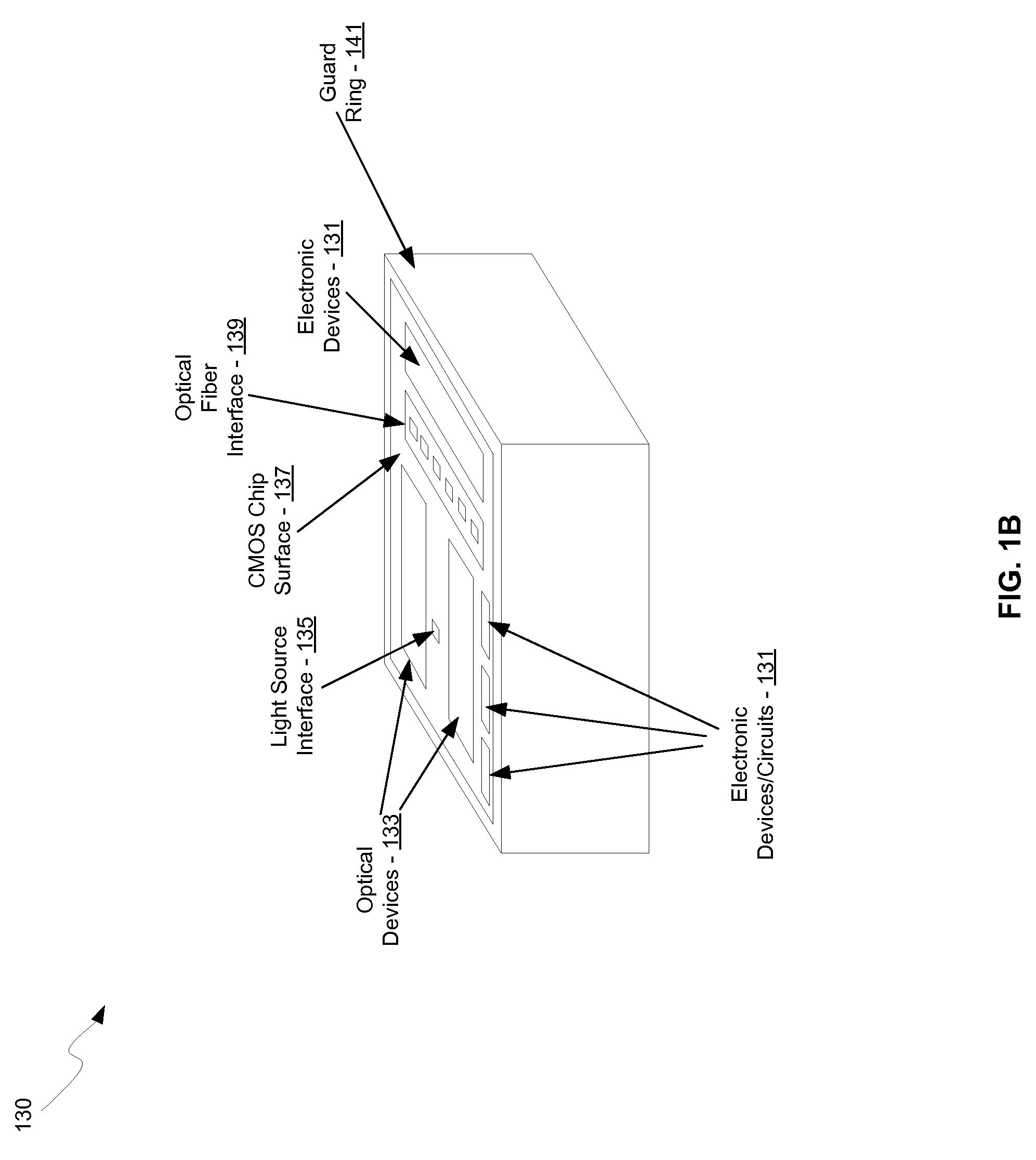
[0021]Certain aspects of the invention may be found in a method and system for split voltage domain receiver circuits. Exemplary aspects of the invention may comprise amplifying complementary received signals in a plurality of partial voltage domains. The signals may be combined into a single differential signal in a single voltage domain. Each of the partial voltage domains may be offset by a DC voltage from the other partial voltage domains. The sum of the partial domains may be equal to a supply voltage of the integrated circuit. The complementary signals may be received from a photodiode. The amplified received signals may be amplified via stacked common source amplifiers, common emitter amplifiers, or stacked inverters. The amplified received signals may be DC coupled prior to combining. The complementary received signals may be amplified and combined via cascode amplifiers. The voltage domains may be stacked, and may be controlled via feedback loops. The photodetector may be i...


PUM


Abstract

Methods and systems for split voltage domain receiver circuits are disclosed and may include amplifying complementary received signals in a plurality of partial voltage domains. The signals may be combined into a single differential signal in a single voltage domain. Each of the partial voltage domains may be offset by a DC voltage from the other partial voltage domains. The sum of the partial domains may be equal to a supply voltage of the integrated circuit. The complementary signals may be received from a photodiode. The amplified received signals may be amplified via stacked common source amplifiers, common emitter amplifiers, or stacked inverters. The amplified received signals may be DC coupled prior to combining. The complementary received signals may be amplified and combined via cascode amplifiers. The voltage domains may be stacked, and may be controlled via feedback loops. The photodetector may be integrated in the integrated circuit.

Description

CROSS-REFERENCE TO RELATED APPLICATIONS / INCORPORATION BY REFERENCE[0001]This application makes reference to and claims priority to U.S. Provisional Application Ser. No. 60 / 997,282 filed on Oct. 2, 2007, which is hereby incorporated herein by reference in its entirety.[0002]This application also makes reference to: U.S. patent application Ser. No. ______ (Attorney Docket No. 19696US01) filed on even date herewith.[0003]Each of the above stated applications is hereby incorporated herein by reference in its entirety.FEDERALLY SPONSORED RESEARCH OR DEVELOPMENT[0004][Not Applicable]MICROFICHE / COPYRIGHT REFERENCE[0005][Not Applicable]FIELD OF THE INVENTION[0006]Certain embodiments of the invention relate to integrated circuit power control. More specifically, certain embodiments of the invention relate to a method and system for split voltage domain receiver circuits.BACKGROUND OF THE INVENTION[0007]Electronic circuits typically require a bias voltage for proper operation. The voltage lev...

Claims


Application Information

Patent Timeline
Patent Type & Authority Applications(United States)
IPC IPC(8): H04B10/06
CPCG02B6/4201H04L25/0272H04B10/564H04B10/516H04B10/501G02B6/4242H04B10/60H04B10/693H04L25/061
Inventor WELCH, BRIAN
Owner CISCO TECH INC
Why Eureka
Try Eureka