Polycrystal collecting area invert structure SiGe hetero-junction transistor

A heterojunction transistor and inverted structure technology, which is applied in semiconductor devices, semiconductor/solid-state device manufacturing, electrical components, etc., can solve the problems of not being able to manufacture high-quality transistors, affecting the high-frequency performance and microwave performance of SiGeHBT, and achieve excellent High frequency performance, effect of reducing process complexity

Inactive Publication Date: 2008-04-16
TSINGHUA UNIV
View PDF0 Cites 11 Cited by
  • Summary
  • Abstract
  • Description
  • Claims
  • Application Information

AI Technical Summary

Problems solved by technology

Precise control is required for the position of the PN junction. Generally, the position of the PN junction should be placed inside the material barrier. If this is not the case, i

Method used


Image

  • Polycrystal collecting area invert structure SiGe hetero-junction transistor
  • Polycrystal collecting area invert structure SiGe hetero-junction transistor

Examples


Embodiment Construction

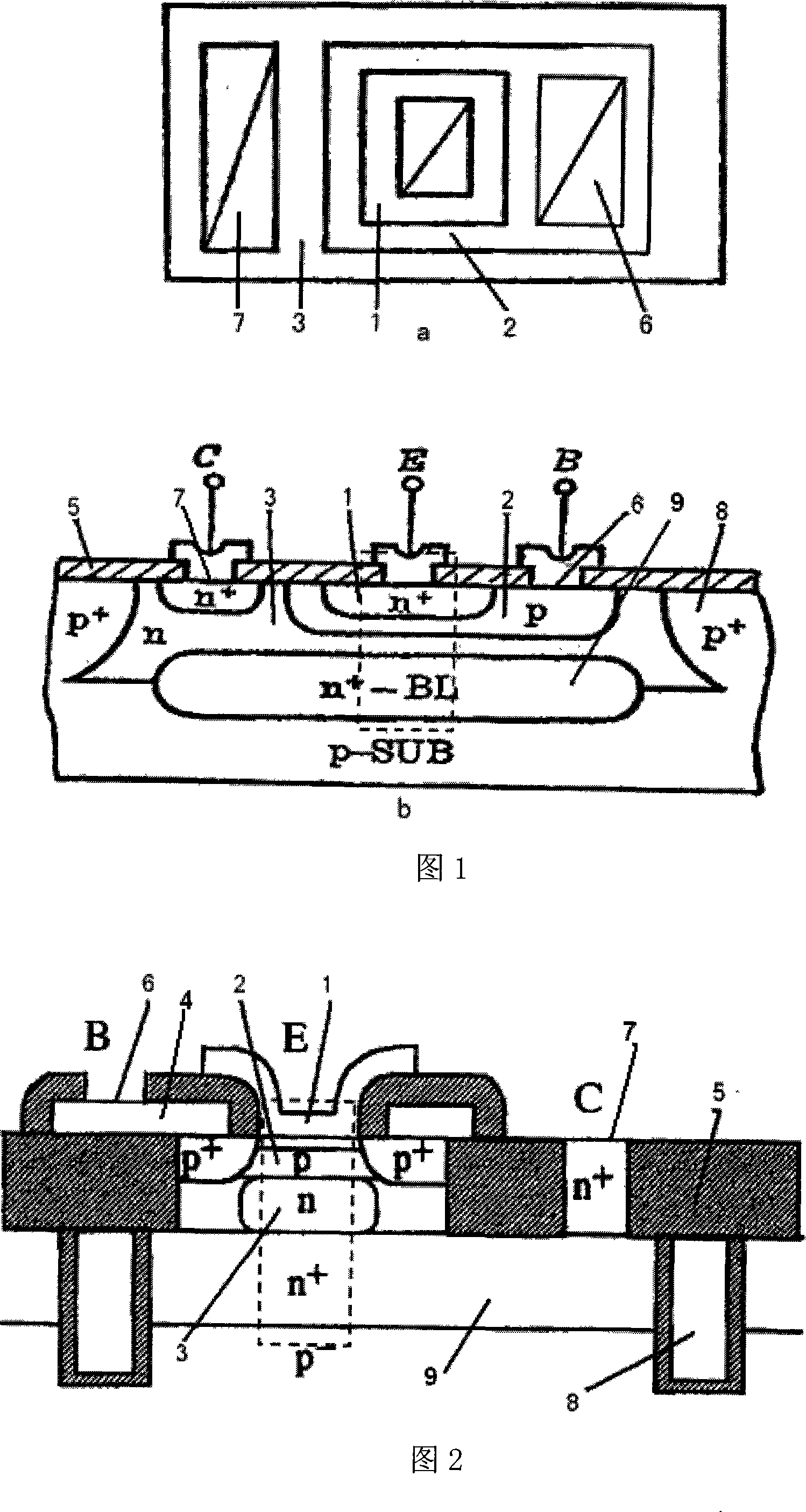
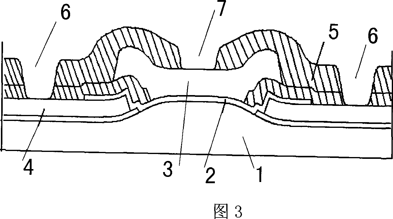
[0040] The invention provides a SiGe heterojunction transistor with an inverted structure in a polysilicon collection area. Its main structure is shown in Figure 3 as the cross-sectional structure of the device.

[0041] The specific production process is illustrated as follows:

[0042] 1) On the substrate silicon wafer, the substrate silicon wafer can be a double-layer structure of P-type plus N+-type Si, or it can be all N+-type. The field oxide layer is grown, typically 1 μm, and then all oxide layers are removed. After this After one-step treatment, the surface presents a slow ups and downs;

[0043] 2) Growth of a thin oxide layer (SiO 2Layer) 5, typically 30nm to 50nm; using LPCVD to deposit polycrystalline Si for base extraction, typically 200nm, and perform P-type doping on the polycrystalline Si;

[0044] 3) RIE plasma dry etching is used to etch away part of the polysilicon, leaving only the part used as the base lead 4; and then wet etching the thin oxide layer ...


PUM

PropertyMeasurementUnit
Thicknessaaaaaaaaaa

Abstract

The invention discloses a SiGe hetero junction transistor with polycrystal collecting region inverted structure, belonging to the semiconductor device structure and fabrication technology field. After avoiding a buried layer and an N- epitaxy Si layer structure in general SiGe HBT transistor, an underlay N+ layer is directly taken as an emitting area, and then a SiGe epitaxy base region, a polycrystal Si collecting area and an electronic device structure consisting of an emitter, a base electrode and a collector are in turn made. The collecting region is positioned on the upper layer of the structure, which contributes to adopting ion injecting technique to adjust the position of B-C junction, thereby well guaranteeing the performance of device. An outside base region and the down-lead of base electrode adopt a dielectric layer to separate from the lower emitting area, which reduces capacitance and guarantees the working speed of device. The transistor with the inverted structure is suitable for forming SiGe microwave monolithic integrated circuit in a form of common emitter.

Description

technical field [0001] The invention belongs to the structure scope of semiconductor devices, in particular to a SiGe heterojunction transistor with an inverted structure in a polysilicon collection area. Background technique [0002] The NPN transistor (NPN triode) fabricated by traditional silicon bipolar process technology is shown in Figure 1. The core device part of the transistor (the part framed by a dotted line in Figure 1), from bottom to top: P-type Si substrate, collection region 3 composed of N+ type Si and N-type Si, P-type Si base region 2. N+ type Si emitter region 1. On this basis, many variants of the NPN transistor structure have been developed. For example, instead of using monocrystalline Si in the emitter region, polycrystalline Si is used instead. Such a structure is shown in Figure 2, which is a currently popular device structure. The transistor shown in Figure 2, its core device part (the part framed by the dotted line in Figure 2), from bottom to t...

Claims


Application Information

Patent Timeline
IPC IPC(8): H01L29/737H01L21/331
Inventor 严利人刘志弘周卫
Owner TSINGHUA UNIV
Why Eureka
Try Eureka