Sequential flow deposition of a tungsten silicide gate electrode film

a gate electrode and flow deposition technology, applied in the field of semiconductor device manufacturing, can solve the problems of large device performance limitation, large change in the effective work function of the relative poor electric conductivity of the polysilicon used for the gate electrode in the gate stack, so as to prevent or cause only small increases in the eot of the gate stack during processing

Inactive Publication Date: 2009-04-02
TOKYO ELECTRON LTD
View PDF31 Cites 4 Cited by
  • Summary
  • Abstract
  • Description
  • Claims
  • Application Information

AI Technical Summary

Benefits of technology

[0007]A method is provided for forming WSix gate electrode films with tunable Si/W atomic ratios for work function control that is suitable for gate stacks in advanced semiconductor devices. According to embodiments of the invention, the silicon/tungsten (Si/W) at...

Problems solved by technology

In semiconductor devices, the relatively poor electric conductivity of polysilicon used for gate electrodes in gate stacks is a major limitation on the device performance.
One difficulty with finding a metal or metal-containing material with the right work function is that the effective work function of a gate stack changes with processing steps required to manufacture ...

Method used


Image

  • Sequential flow deposition of a tungsten silicide gate electrode film
  • Sequential flow deposition of a tungsten silicide gate electrode film
  • Sequential flow deposition of a tungsten silicide gate electrode film

Examples


example 1

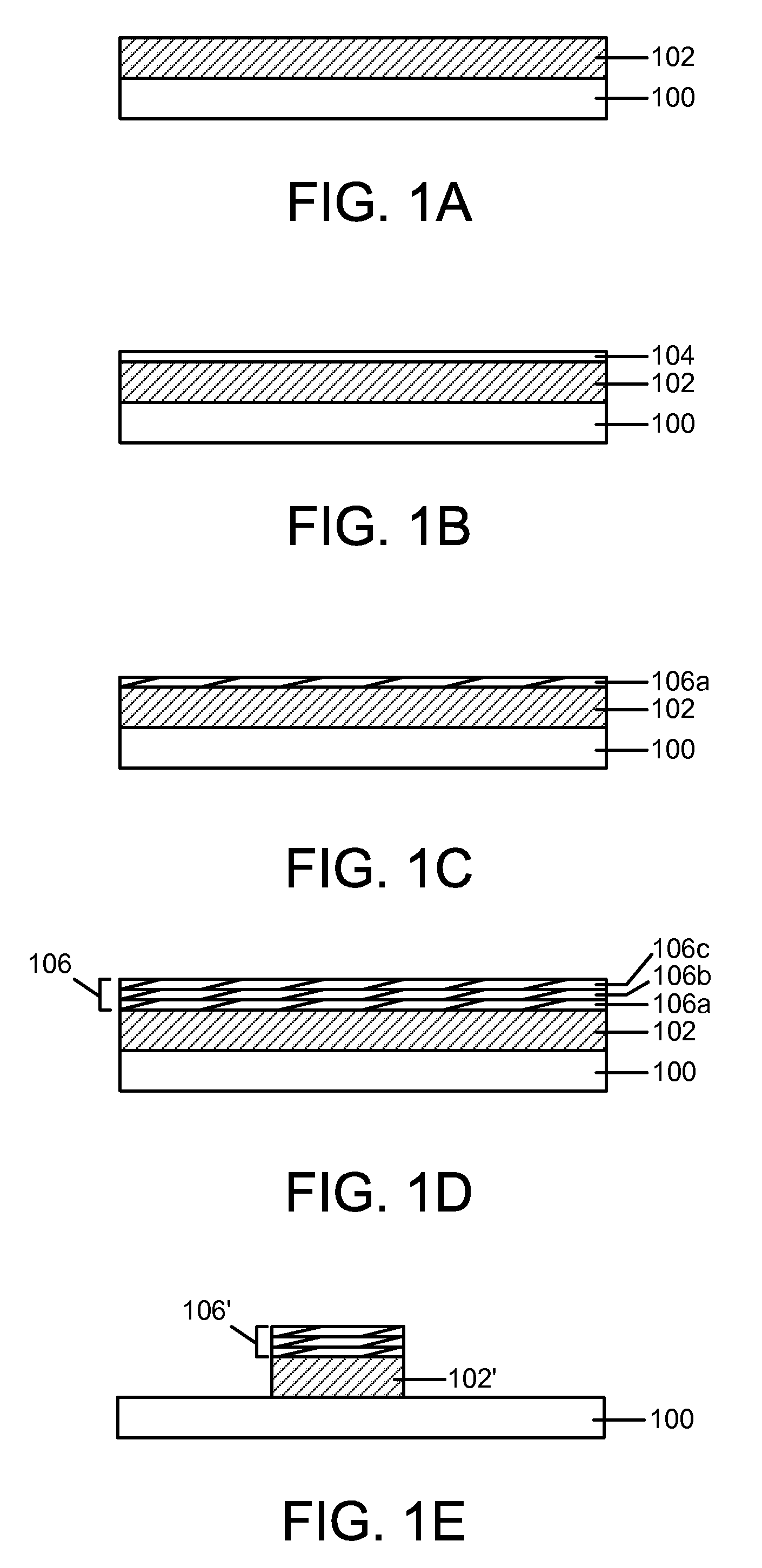
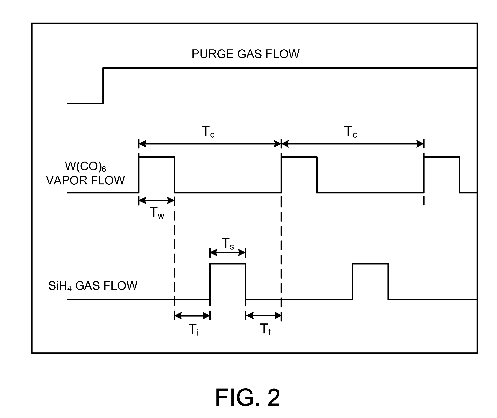
[0033]A WSix gate electrode film 106 with a Si / W atomic ratio of 0.76 was formed on a high-k film 102 by sequential flow deposition using a first process gas containing W(CO)6 vapor and Ar gas, a second process gas containing undiluted SiH4 gas, continuous flow of Ar purge gas, and substrate temperature of 500° C. A 2 nm thick W metal film 104 was deposited in each deposition cycle using Tw=11 sec, and a gas pressure of 220 mTorr in the process chamber during time periods Tw and Tf. The length of each time period Ts, Ti, and Tf was 12 sec and the gas pressure was maintained at 500 mTorr during time periods Ti and Ts. During time period Ti, the W metal film 104 was exposed to Ar purge gas and SiH4 gas and during time period Ti, the WSix film was exposed to Ar purge gas only. The O film impurity in the WSix gate electrode film 106 was 16.7%.

example 2

[0034]A WSix gate electrode film 106 with a Si / W atomic ratio of 2.6 was formed on a high-k film 102 by sequential flow deposition using a first process gas containing W(CO)6 vapor and Ar gas, a second process gas containing undiluted SiH4 gas, continuous flow of Ar purge gas, and substrate temperature of 500° C. A 1 nm thick W metal film 104 was deposited in each deposition cycle using Tw=5 sec, and a gas pressure of 220 mTorr in the process chamber during time periods Tw and Tf. The length of each time period Ts, Ti, and Tf was 12 sec and the gas pressure was maintained at 500 mTorr during time periods Ti and Ts. During time period Ti, the W metal film 104 was exposed to Ar purge gas and SiH4 gas and during time period Ti, the WSix film was exposed to Ar purge gas only. The O film impurity in the WSix gate electrode film 106 was 2.9%.

example 3

[0035]A WSix gate electrode film 106 with a Si / W atomic ratio estimated at 3.5-4 was formed on a high-k film 102 by sequential flow deposition using a first process gas containing W(CO)6 vapor and Ar gas, a second process gas containing undiluted SiH4 gas, continuous flow of Ar purge gas, and substrate temperature of 500° C. A 0.5 nm thick W metal film 104 was deposited in each deposition cycle using Tw=3 sec, and a gas pressure of 220 mTorr in the process chamber during time periods Tw and Tf. The length of each time period Ts, Ti, and Tf was 12 sec and the gas pressure was maintained at 500 mTorr during time periods Ti and Ts. During time period Ti, the W metal film 104 was exposed to Ar purge gas and SiH4 gas and during time period Ti, the WSix film was exposed to Ar purge gas only. The O film impurity in the WSix gate electrode film 106 was <2.9%.

[0036]As shown in Examples 1-3 above, the Si / W atomic ratio of a WSix gate electrode film 106 was varied from about 0.76 to about 3.5-...


PUM

PropertyMeasurementUnit
Temperatureaaaaaaaaaa

Abstract

A method is provided for forming WSix gate electrode films with tunable Si/W atomic ratios, low oxygen and carbon film impurities, and work functions suitable for advanced semiconductor devices. The method includes providing a substrate containing a high-k film in a process chamber, maintaining the substrate at a temperature between 450° C. and 550° C., and performing a plurality of deposition cycles to form a WSix gate electrode film on the high-k film. According to embodiments of the invention, each deposition cycle includes exposing the substrate to a first process gas containing W(CO)6 vapor to thermally deposit a W metal film with a thickness between 0.1 nm and less than 2 nm, and exposing the W metal film to a second process gas containing SiH4 to form a WSix film having a Si/W atomic ratio controlled by self-limited Si incorporation into the W metal film. The method further includes patterning the WSix gate electrode film and high-k film to form a gate stack.

Description

CROSS-REFERENCE TO RELATED APPLICATION[0001]This application is related to co-pending U.S. patent application Ser. No. 10 / 673,910, entitled METHOD FOR DEPOSITING METAL LAYERS USING SEQUENTIAL FLOW DEPOSITION and filed on Sep. 30, 2003, the entire content of which is incorporated herein by reference. The related application is not commonly-owned.FIELD OF INVENTION[0002]The field of the invention relates generally to the field of semiconductor device manufacturing and, more specifically, to formation of a tungsten silicide (WSix) gate electrode film with tunable tungsten to silicon ratios, low carbon and oxygen film impurities, and work functions that are suitable for advanced semiconductor devices.BACKGROUND OF THE INVENTION[0003]In semiconductor devices, the relatively poor electric conductivity of polysilicon used for gate electrodes in gate stacks is a major limitation on the device performance. The need for replacing polysilicon with a low resistivity material with high stability...

Claims


Application Information

Patent Timeline
IPC IPC(8): C23C16/06
CPCC23C16/45525C23C16/42
Inventor LEUSINK, GERRIT J.GUIDOTTI, EMMANUAL P.
Owner TOKYO ELECTRON LTD
Why Eureka
Try Eureka