Directed Assembly of Carbon Nanotubes and Nanoparticles Using Nanotemplates With Nanotrenches

a technology of carbon nanotubes and nanoparticles, applied in the field of nanoscience and nanotechnology, can solve the problems of limited nanotools and fabrication methods for their assembly, inefficient and tedious, and the manipulation of individual nanoelements, and achieve the effect of high electrical and thermal conductivity and high strength

Active Publication Date: 2009-04-02
NORTHEASTERN UNIV
View PDF16 Cites 58 Cited by
  • Summary
  • Abstract
  • Description
  • Claims
  • Application Information

AI Technical Summary

Problems solved by technology

Although carbon nanotubes have been assembled into different nanostructures, only limited nanotools and fabrication methods for their assembly have been developed.
One obstacle has been the manipulation of individual nanoelements, which is often inefficient and tedious.
This problem is particularly challenging when assembling complex nanostructures that require selecting and ordering millions of nanoelements across a large area.
Although these methods are useful for fabricating simple nanodevices, neither is practical when selecting and patterning, for example, millions of nanoelements for more complex structures.
These methods, however, remain incapable of manipulating individual nanoelements.
The development of nanomachines or “nanoassemblers” which are programmed and used to order nanoelements for their assembly holds promise, although there have been few practical advancements with these machines.
Self-assembled monolayers, however, have been problematic when used to transfer nanoelements from one nanosubstrate to a recipient substrate.
Although particle interactions can be modified to affect their transport, optical and electrical properties, controlling nanoelement orientation is also a challenge in self-assembly methods.
Similarly, nanoscience has been incapable of manipulating particle interactions to reproducibly assemble hundreds of nanodevices.
Previously available methods such as those mentioned above have yet to meet these requirements.
The hindrance to the realization of electronic circuits with carbon nanotubes is the difficulty in positioning and contacting them in a controlled way on a large scale.
These techniques, however, are not suitable for large scale controlled assembly of carbon nanotubes and other nanoelements.
Previous attempts to direct the assembly process using DC electrophoresis with nanowires have failed.

Method used


Image

  • Directed Assembly of Carbon Nanotubes and Nanoparticles Using Nanotemplates With Nanotrenches
  • Directed Assembly of Carbon Nanotubes and Nanoparticles Using Nanotemplates With Nanotrenches
  • Directed Assembly of Carbon Nanotubes and Nanoparticles Using Nanotemplates With Nanotrenches

Examples


example i

Manufacturing a Nanosubstrate for Carbon Nanotube Assembly

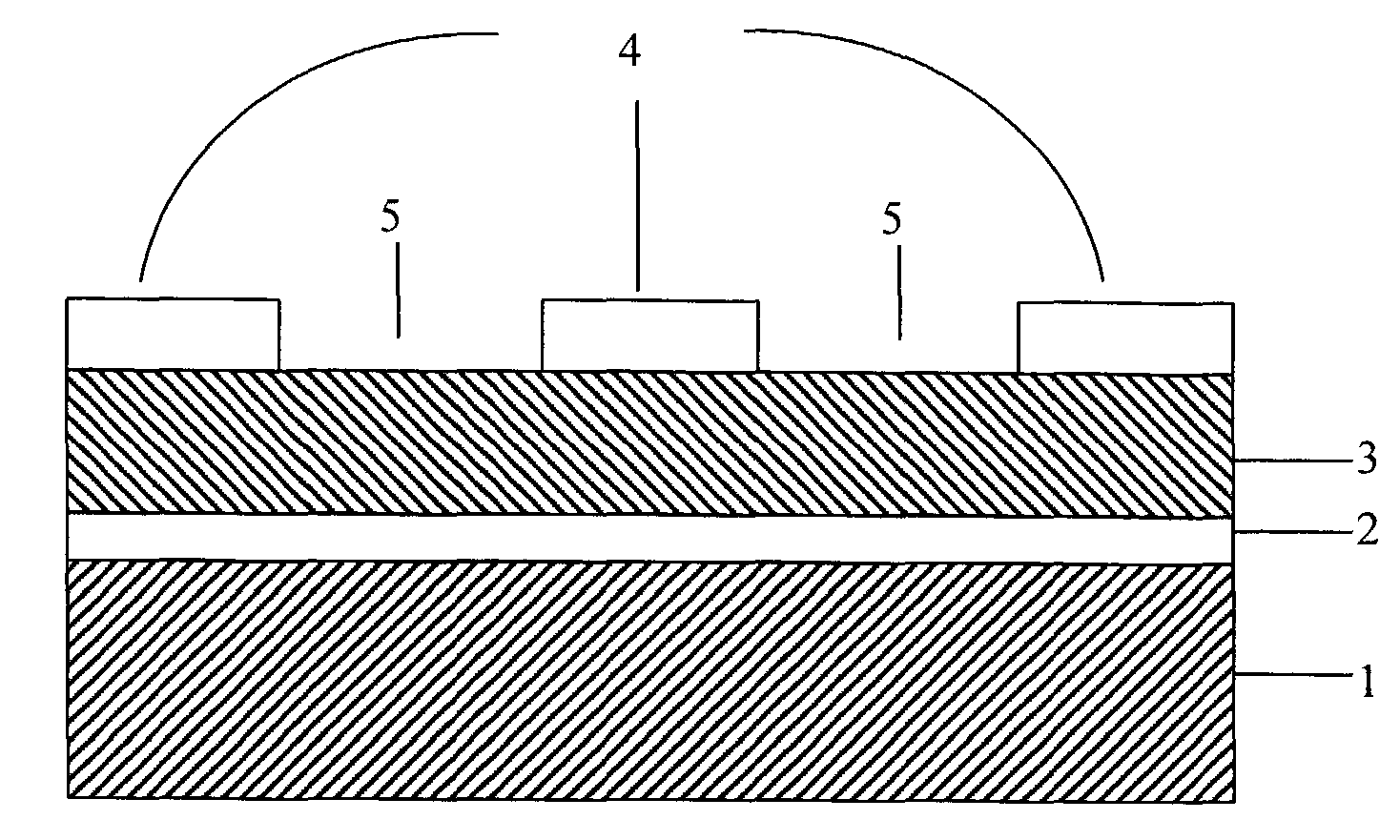
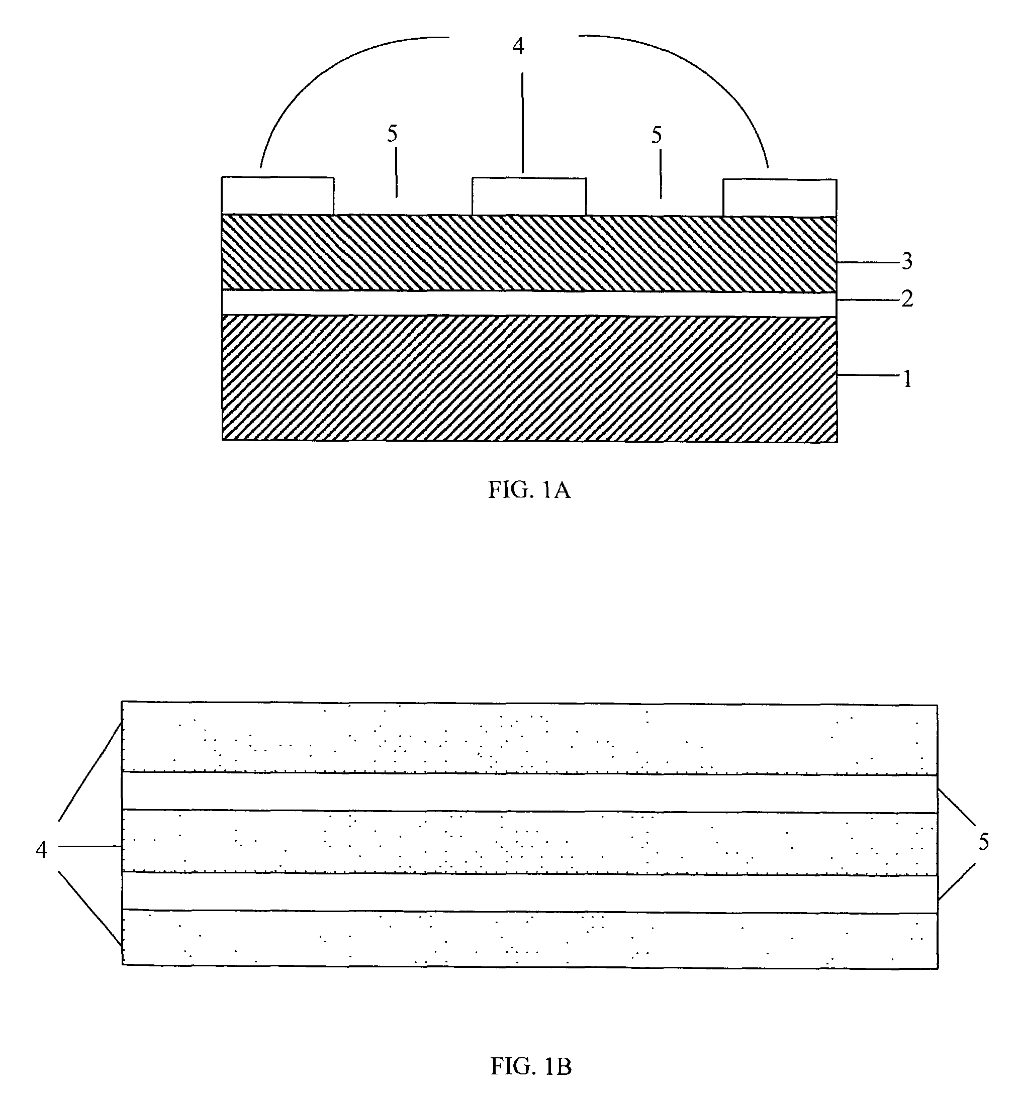
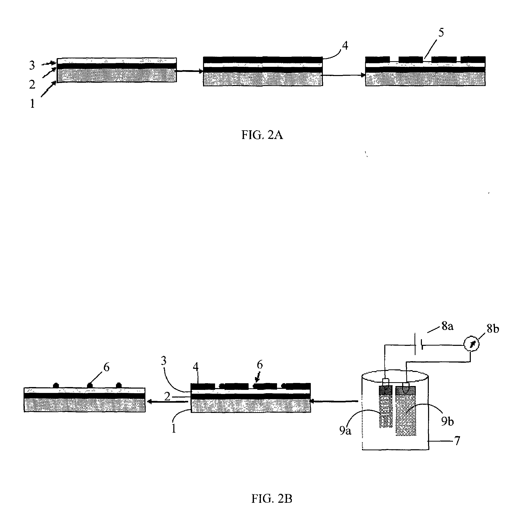
[0052]A 5 nm layer of Cr was deposited by sputtering onto an oxidized silicon surface. A 50 nm layer of Au was then deposited by sputtering over the Cr layer. A 150 nm thick PMMA layer was then spun over the surface. Electron beam lithography was used to pattern nanotrenches of various sizes (see subsequent examples) in the PMMA layer. Following exposure, the substrate was developed resulting in the formation of nanotrenches on the PMMA film exposing parts of the gold surface.

example ii

Assembly of Carbon Nanotube Bundles

[0053]The nanosubstrate from Example I was immersed in a 10 ml suspension of 0.01 wt / vol % single wall carbon nanotubes (SWNT) in deionized water. The SWNT were obtained from Carbon Nanotechnologies, Inc. (Houston, Tex.). The pH of the solution was adjusted to 8 by adding ammonium hydroxide solution (final concentration approximately 1 μM). A clean gold substrate placed at a distance of 1 centimeter from the PMMA substrate acted as the cathode. A DC voltage was applied between the two electrodes for 60 seconds, and the current was monitored using a pico-ammeter. An electric field of either 5 V / cm (FIG. 3A) or 3 V / cm (FIG. 3C) resulted in the negatively charged nanotubes being assembled inside the trenches wherever the gold layer was exposed. There were some nanotubes protruding out of the trench, especially at the edges, but these were removed after the PMMA was dissolved (see below).

[0054]Following assembly, the PMMA film was stripped using aceton...

example iii

Effect of Trench Width on Assembly of Carbon Nanotubes

[0056]To investigate the effect of trench width on assembly, nanosubstrates were fabricated with 70 μm long trenches having widths of approximately 350 nm, 250 nm, 150 nm, 100 nm and 50 nm. As seen from the results presented in FIGS. 4-7, the density of nanotubes assembled inside the trenches decreased with the width of the trenches for a given voltage.


PUM

PropertyMeasurementUnit
lengthaaaaaaaaaa
diameteraaaaaaaaaa
widthaaaaaaaaaa

Abstract

The present invention provides methods and tools for directed assembly of nanoelements across a large area using a nanosubstrate. The nanosubstrate has a substrate layer, an adhesive layer, a conductive layer, and an insulating layer that is interrupted by one or more nanotrenches or nanowells having a width of at least 20 nm. The nanosubstrate allows the rapid assembly of linear assemblies and arrays of single walled carbon nanotubes and nanoparticles by DC electrophoresis. The density of nanoelements assembled can be controlled by varying the voltage and trench size. Functionalized nanoparticles can be assembled into arrays useful, e.g., as biosensors.

Description

CROSS REFERENCE TO RELATED APPLICATIONS[0001]This application claims the priority of U.S. Provisional Application No. 60 / 741,421 filed Dec. 1, 2005 and entitled, DIRECTED ASSEMBLY OF CARBON NANOTUBES AND NANOPARTICLES USING NANOTEMPLATES WITH NANO-TRENCHES OR NANOWIRES, which is hereby incorporated by reference herein.STATEMENT REGARDING FEDERALLY SPONSORED RESEARCH[0002]The invention was made with support from Grant EEC-0425826 from the National Science Foundation Nanoscale Science and Engineering Center. The United States Government has certain rights in the invention.BACKGROUND OF THE INVENTION[0003]The fields of nanoscience and nanotechnology generally concern the synthesis, fabrication and use of nanoelements and nanostructures at atomic, molecular and supramolecular levels. The nanosize of these elements and structures offers significant potential for research and applications across the scientific disciplines, including materials science, physics, chemistry, computer science,...

Claims


Application Information

Patent Timeline
Patent Type & Authority Applications(United States)
IPC IPC(8): C07K1/26B32B9/00G03F7/20
CPCB81B2201/0214B81C1/00031B81C1/00206B82B3/00B82Y30/00Y10T428/2918C01B31/0253C01B2202/34C01B2202/36Y10T428/2462B82Y40/00C01B32/168
Inventor BUSNAINA, AHMEDMCGRUER, NICOL E.
Owner NORTHEASTERN UNIV
Why Eureka
Try Eureka