Semiconductor device having high frequency wiring and dummy metal layer at multilayer wiring structure
a technology of high frequency wiring and multi-layer wiring structure, which is applied in the direction of semiconductor devices, semiconductor/solid-state device details, diodes, etc., can solve the problems of increased parasitic capacity components of inductor and transformer, ineffective prevention of erosion, etc., and achieve the effect of improving the characteristics of semiconductor devices and preventing erosion and dishing
- Summary
- Abstract
- Description
- Claims
- Application Information
AI Technical Summary
Benefits of technology
Problems solved by technology
Method used
Image
Examples
first exemplary embodiment
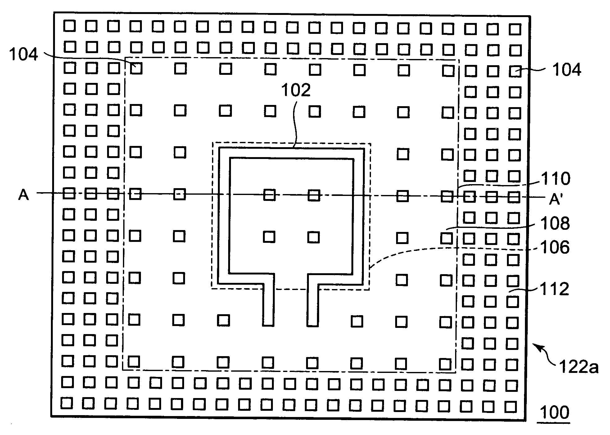
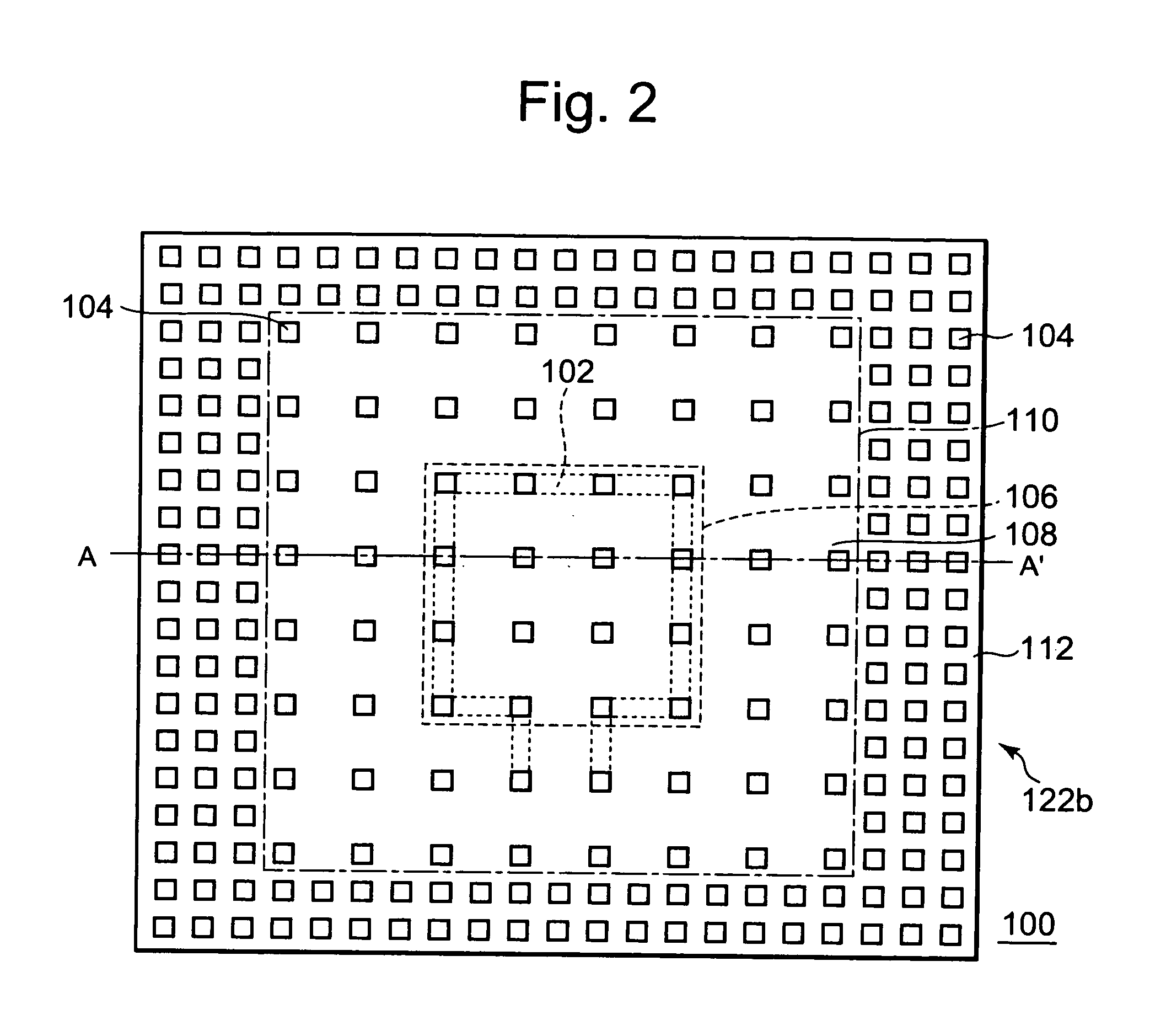
[0025]FIGS. 1 and 2 are top views showing a configuration of a semiconductor device 100 in this first exemplary embodiment respectively. FIG. 3 is a cross sectional view taken on line A-A′ of FIGS. 1 and 2.
[0026]FIG. 1 is a top view of a first wiring layer 122a (first layer) provided with a high frequency wiring 102 and FIG. 2 is a top view of one of second wiring layers 122b (second layer) provided between the first wiring layer 122a and the semiconductor substrate 120. In FIG. 2, a dotted line shows a region superposed on the high frequency wiring 102 at a top view. The high frequency wiring 102 is formed in a coil pattern at a top view and functions as an inductor or transformer. In the high frequency wiring flown a current having a frequency of, for example, 5 GHz or higher. Dummy metals 104 are provided for the first wiring layer 122a and for each of the second wiring layers 122b. A dummy metal means a conductive pattern which substantially does not affect the circuit provided ...
second exemplary embodiment
[0043]In this second exemplary embodiment, a guard ring 116 is provided between a vicinity region 110 surrounding the high frequency wiring 102 and the external region 112. This makes a difference between the semiconductor device in this second embodiment and that 100 in the first embodiment described with reference to FIGS. 1 through 3. The high frequency wiring 102 may be an inductor.
[0044]FIGS. 5 and 6 are top views of the configuration of a semiconductor device 100 in this second exemplary embodiment. FIG. 7 is a cross sectional view taken on line B-B′ of FIG. 6. FIG. 5 is a top view of the first wiring layer 122a (first layer) having the high frequency wiring 102. FIG. 6 is a top view of the second wiring layer 122b (second layer) provided between the first wiring layer 122a and the semiconductor substrate 120.
[0045]As shown in FIG. 7, the guard ring 116 can be formed as a continuous element through all the layers of the multilayer wiring layer 122. Although not limited special...
PUM
 Abstract
Description
Claims
Application Information


