Cof board

a technology of cof board and cof plate, which is applied in the direction of printed circuit, sustainable manufacturing/processing, final product manufacturing, etc., can solve the problems of easy cause of gap and degradation of connection reliability, and achieve excellent connection reliability and prevent density unevenness

Inactive Publication Date: 2009-04-16
NITTO DENKO CORP
View PDF4 Cites 8 Cited by
  • Summary
  • Abstract
  • Description
  • Claims
  • Application Information

AI Technical Summary

Benefits of technology

[0010]It is an object of the present invention to provide a COF board which can be increased in density, and also has high connection reliability.
[0015]In the COF board of the present invention, the terminal portion includes the first lead, and the second lead having the length in the longitudinal direction smaller than the length of the first lead in the longitudinal direction. The plurality of first leads are arranged in spaced-apart relation in the direction perpendicular to the longitudinal direction. The plurality of second leads are arranged in the direction perpendicular to the longitudinal direction to be interposed between the mutually adjacent first leads such that, when the mutually adjacent first leads are projected in the adjacent direction thereof, the overlap portion where the second leads overlap with the first leads and the non-overlap portions where the second leads do not overlap with the first leads are formed. As a result, a level difference along the direction perpendicular to the longitudinal direction is formed between the first lead and the second lead to allow an increase in the density of the terminal portions.
[0016]On the other hand, the dummy leads are provided at the non-overlap portions of the COF board. Therefore, in the formation of the terminal portions by electrolytic plating, it is possible to prevent density unevenness of the first leads and the second leads with respect to a plating solution, and substantially equalize the concentration of metal ions in the plating solution in the vicinity of the first lead, and the concentration of metal ions in the plating solution in the vicinity of the overlap portion between the dummy lead and the second lead. This allows the first lead and the second lead to have equal thicknesses. As a result, it is possible to unify the thickness of the terminal portion, and obtain excellent connection reliability.
[0017]Further, since the dummy leads are provided at the non-overlap portions of the COF board, the COF board can be reinforced when the electronic component is mounted thereon.

Problems solved by technology

That is, density unevenness of the leads with respect to the plating solution are caused, so that the concentration of metal ions in the plating solution is higher in the vicinities of the longer terminal end portions than in the vicinities of the shorter terminal end portions.
When a semiconductor element is mounted on such terminal portions, a gap is easily caused between the thinner shorter terminal end portions and the connection terminal of the semiconductor element.
This leads to defective connection to cause degradation of connection reliability.

Method used


Image

  • Cof board
  • Cof board
  • Cof board

Examples


example 1

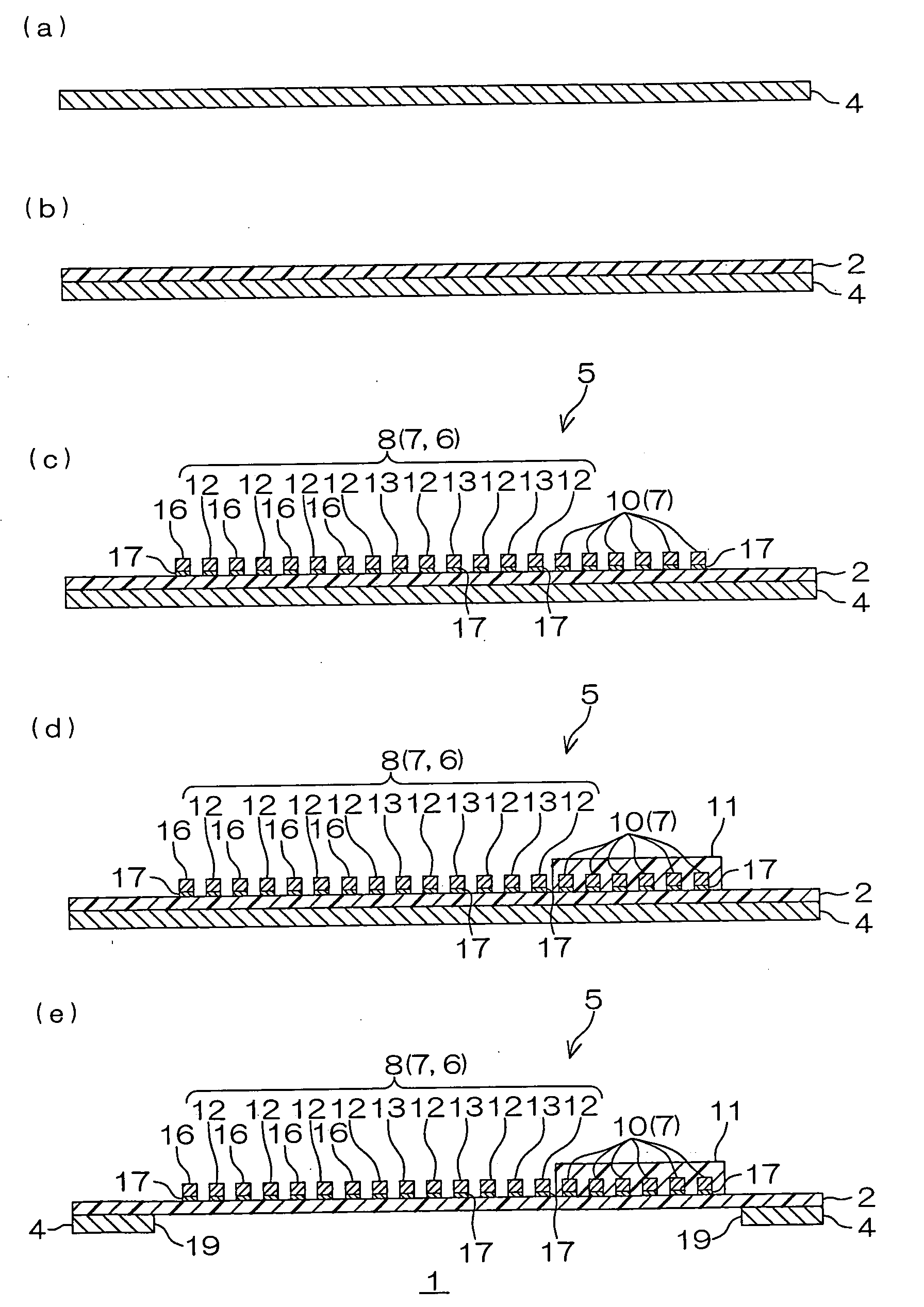
[0089]A reinforcing layer made of a stainless steel foil having a thickness of 20 μm was prepared (see FIG. 5(a)). Then, a solution of a polyamic acid resin was coated on the entire surface of the reinforcing layer, dried, exposed to light, developed, and then cured by heating to form an insulating base layer made of a polyimide resin and having a thickness of 25 μm (see FIG. 5(b)).

[0090]Then, conductive patterns and dummy leads were simultaneously formed by an additive method.

[0091]That is, a chromium thin film having a thickness of 30 nm and a copper thin film having a thickness of 200 nm were formed in this order by a sputtering method to form a metal thin film. Then, on the metal thin film, a plating resist made of a dry film resist was formed in a pattern reverse to the conductive patterns, and to a pattern of the dummy leads. Thereafter, the conductive patterns and the dummy leads were formed on the metal thin film exposed from the plating resist by electrolytic copper plating...

examples 2 to 5

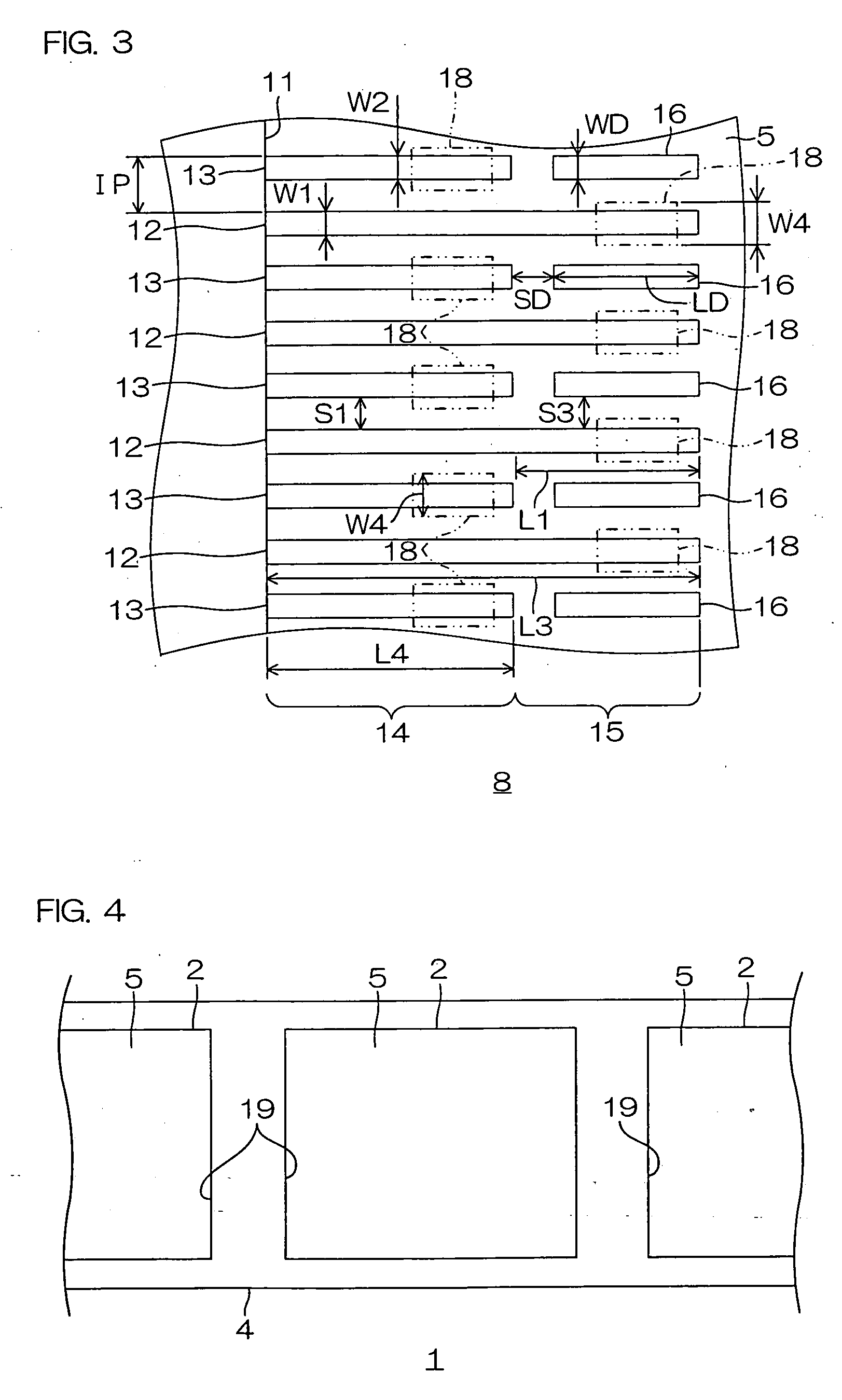
[0095]COF boards of EXAMPLES 2 to 5 were obtained in the same manner as in EXAMPLE 1 except that the dimensions of the inner leads and the dummy lead were changed as shown below in Table 1 in the formation of the conductive patterns.


PUM


Abstract

A COF board includes an insulating layer, and a terminal portion formed on the insulating layer. The terminal portion includes a first lead extending in a longitudinal direction, and a second lead extending in the longitudinal direction, and having a smaller length in the longitudinal direction than a length of the first lead in the longitudinal direction. The first leads are arranged in spaced-apart relation in a direction perpendicular to the longitudinal direction. The second leads are arranged in the direction perpendicular to the longitudinal direction to be interposed between the mutually adjacent first leads such that, when the mutually adjacent first leads are projected in an adjacent direction thereof, overlap portions where the second leads overlap with the first leads and non-overlap portions where the second leads do not overlap with the first leads are formed. Dummy leads are provided at the non-overlap portions.

Description

CROSS-REFERENCE TO RELATED APPLICATION[0001]The present application claims priority from Japanese Patent Application No. 2007-264797, filed on Oct. 10, 2007, the content of which is hereby incorporated by reference in its entirety.BACKGROUND OF THE INVENTION[0002]1. Field of the Invention[0003]The present invention relates to a COF board and, more particularly, to a COF board for mounting an electronic component.[0004]2. Description of the Related Art[0005]On a COF board, an electronic component such as a semiconductor element (an IC chip and the like) is nakedly mounted (bare-chip mounted) without being contained in a package by a COF (Chip on film) method. The COF board is mounted on various electronic equipment. The COF board typically includes an insulating base layer, and terminal portions formed thereon to be connected to the connection terminals of the electronic component.[0006]As electronic equipment has been increasingly reduced in thickness, length, and width in recent ye...

Claims


Application Information

Patent Timeline
Patent Type & Authority Applications(United States)
IPC IPC(8): H01L23/495
CPCH01L23/49838H01L23/4985H05K1/056H05K1/111H05K1/189H05K2201/09709H01L2924/0002H05K2201/09781H05K2201/10674H05K2203/1545H01L2924/00Y02P70/50
Inventor ISHIMARU, YASUTOEBE, HIROFUMI
Owner NITTO DENKO CORP
Why Eureka
Try Eureka