Semiconductor device and method for fabricating the same

a technology of semiconductor devices and semiconductors, applied in semiconductor devices, semiconductor/solid-state device details, electrical apparatus, etc., can solve the problems of not reducing the reliability of interconnects, and achieve the effect of increasing the effective permittivity, preventing the increase of the variation of the width of the interconnect, and reliably forming

Active Publication Date: 2009-04-16
PANNOVA SEMIC
View PDF10 Cites 49 Cited by
  • Summary
  • Abstract
  • Description
  • Claims
  • Application Information

AI Technical Summary

Benefits of technology

[0042]As has been described, in a semiconductor device according to the present invention, a cap film formed of metal or a material containing metal is provided on each interconnect. Thus, increase in the effective permittivity between adjacent interconnects and also increase in variation in interconnect width can be prevented.
[0043]Moreover, in a method for fabricating a semiconductor device according to the present invention, gas cluster ion beam processing is used for forming nano holes (gaps). Thus, nano holes can be reliably formed and deficiencies in pattern formation caused by differences in light reflectivity and reduction in reliability of interconnects due to etching can be prevented.

Problems solved by technology

Therefore, the reliability of the interconnects is not reduced.

Method used


Image

  • Semiconductor device and method for fabricating the same
  • Semiconductor device and method for fabricating the same
  • Semiconductor device and method for fabricating the same

Examples


first embodiment

[0051]A first embodiment of the present invention will be described with reference to the accompanying drawings.

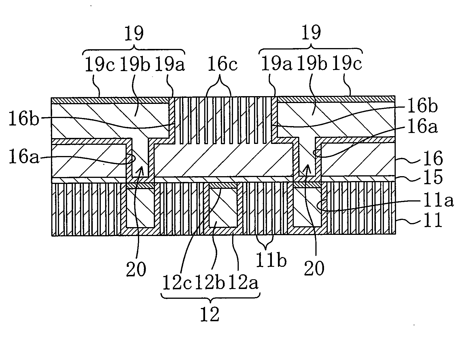
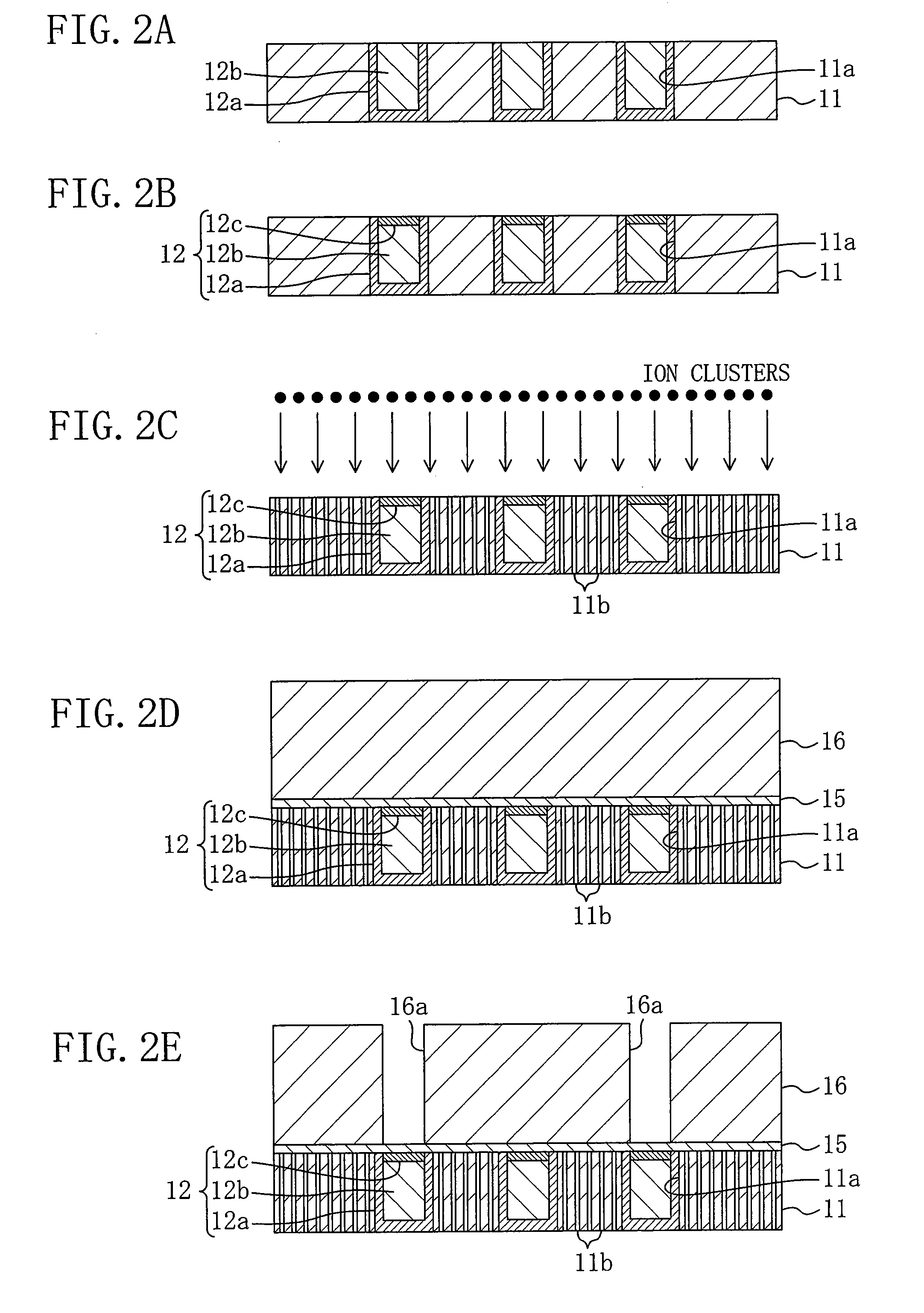
[0052]FIG. 1 is a cross-sectional view illustrating major part (interconnect part) of a semiconductor device according to a first embodiment of the present invention. As shown in FIG. 1, a plurality of lower layer interconnects 12 are selectively formed in a first interlevel insulation film 11.

[0053]Each of the lower layer interconnects 12 is formed of a first barrier metal film 12a of a stacked layer film of tantalum (Ta) and tantalum nitride (TaN) on bottom and wall surfaces of a lower layer interconnect groove 11a formed in the first interlevel insulation film 11, a first copper film 12b provided on the first barrier metal film 12a to fill the lower layer interconnect groove 11 and a first cap film 12c formed of metal or a material containing metal in upper part of the first copper film 12b.

[0054]An insulation material having a small mechanical strength (relative permi...

second embodiment

[0079]Hereafter, a second embodiment of the present invention will be described with reference to the accompanying drawings.

[0080]FIG. 4 is a cross-sectional view illustrating a cross section of major part of a semiconductor device according to the second embodiment of the present invention. In FIG. 4, each member also shown in FIG. 1 is identified by the same reference numeral and therefore the description thereof will be omitted.

[0081]As shown in FIG. 4, a semiconductor device according to the second embodiment is characterized in that an interlevel insulation film formed on a first interlevel insulation film 11 is made to have a two-layer structure including a second interlevel insulation film 16A having a relatively high mechanical strength (relative permittivity) such as, for example, silicon oxide, and a third interlevel insulation film 18 having a lower mechanical strength (relative permittivity) than that of the second interlevel insulation film 16A, such as, for example, a ...

third embodiment

[0087]Hereafter, a third embodiment of the present invention will be described with reference to the accompanying drawings.

[0088]FIG. 5 is a cross-sectional view illustrating a cross section of major part of a semiconductor device according to the third embodiment of the present invention. In FIG. 5, each member also shown in FIG. 1 is identified by the same reference numeral and therefore the description thereof will be omitted.

[0089]FIG. 5 is a cross-sectional view illustrating a cross section of major part of a semiconductor device according to the third embodiment of the present invention. As shown in FIG. 5, the semiconductor device of the third embodiment is characterized in that a cap film 12c having the function of preventing a copper diffusion is provided in upper part of each of lower layer interconnects 12 and a second interlevel insulation film 16 is directly in contact with the first interlevel insulation film 11 and the lower layer interconnects 12.

[0090]Specifically, ...


PUM


Abstract

A semiconductor device includes: a first insulation film formed over a semiconductor substrate; and a plurality of first interconnects selectively formed in the first insulation film. A plurality of gaps are formed in part of the first insulation film located between adjacent ones of the first interconnects so that each of the gaps has a cylindrical shape extending vertically to a principal surface of the semiconductor substrate. A cap film is formed of metal or a material containing metal in upper part of each of the first interconnects.

Description

CROSS-REFERENCE TO RELATED APPLICATION[0001]The disclosure of Japanese Patent Application No. 2007-265248 filed on Oct. 11, 2007, including specification, drawings and claims is incorporated herein by reference in its entirety.BACKGROUND OF THE INVENTION[0002]The present invention relates to a semiconductor device and a method for fabricating the semiconductor device, and more particularly relates to a semiconductor device having an interconnect structure including air gaps and a method for fabricating the semiconductor device.[0003]In recent years, in order to increase the operation speed of semiconductor devices, application of an air gap interconnect structure to semiconductor device fabrication processes has been examined. Normally, for RC delays (i.e., delays generated from resistive components and capacitive components) of an interconnect, a delay generated from capacitive components is determined by a relative permittivity of an insulation film located around the interconnect...

Claims


Application Information

Patent Timeline
Patent Type & Authority Applications(United States)
IPC IPC(8): H01L23/48H01L21/4763
CPCH01L21/7682H01L21/76867H01L21/76849H01L21/76823
Inventor IWASAKI, AKIHISA
Owner PANNOVA SEMIC
Why Eureka
Try Eureka