Inverted OLED device with improved efficiency

a technology of inverted oled and efficiency, which is applied in the manufacture of electrode systems, electric discharge tubes/lamps, discharge tubes luminescent screens, etc., can solve the problems of difficulty in achieving the desired luminance, the voltage rise over time can be very large in the inverted structure, and the device has not performed very well, so as to reduce the rise of the drive voltage with time.

Active Publication Date: 2009-04-16
GLOBAL OLED TECH
View PDF8 Cites 19 Cited by
  • Summary
  • Abstract
  • Description
  • Claims
  • Application Information

AI Technical Summary

Benefits of technology

[0008]It is therefore an object of the present invention to provide an inverted OLED device, which shows a reduced rise in drive voltage with time.

Problems solved by technology

However, these devices have not performed very well due to poor or inadequate injection of holes and electrons at the anode and cathode interfaces, respectively.
In particular, voltage rise over time can be very large in inverted structures.
This produces difficulties in achieving desired luminance.

Method used


Image

  • Inverted OLED device with improved efficiency
  • Inverted OLED device with improved efficiency
  • Inverted OLED device with improved efficiency

Examples


example 2 (

Inventive)

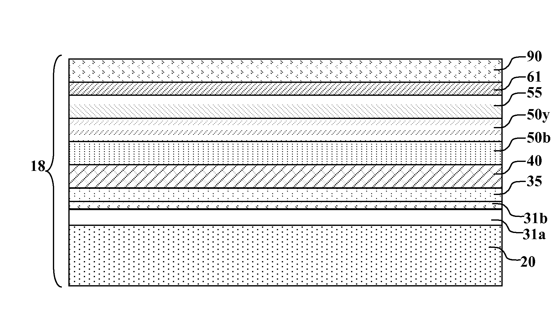
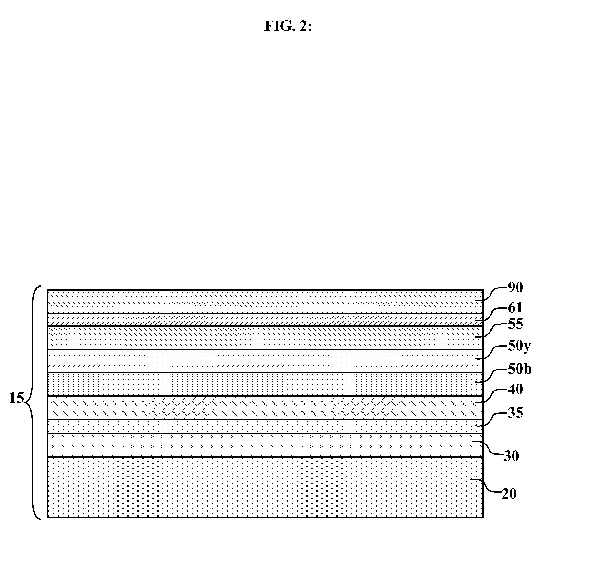
[0123]An inventive bottom-emitting inverted OLED device was constructed in the following manner:[0124]1. A clean glass substrate was deposited by sputtering with ITO to form a transparent cathode of 85 nm thickness.[0125]2. The above-prepared substrate was further treated by vacuum-depositing a 10 nm layer of CHATP as a second electron-accepting layer.[0126]3. A 40 nm mixed electron-transporting layer was vacuum-deposited, including 49% Bphen, 49% ALQ as co-host, with 2% Li metal.[0127]4. The above-prepared substrate was further treated by vacuum-depositing a 20 nm blue light-emitting layer including 92% NBA host and 7% NPB co-host with 1% tetra-t-butylperylene (TBP) as blue-emitting dopant.[0128]5. The above-prepared substrate was further treated by vacuum-depositing a 20 nm yellow light-emitting layer of 68% NPB (as host) and 30% NBA (as co-host) with 2% PTBR.[0129]6. The above-prepared substrate was further treated by vacuum-depositing a 10 nm layer of NPB as a hole-tra...

example 3 (

Inventive)

[0132]An inventive top-emitting inverted OLED device was constructed as described above for Example 2, except that Steps 1, 3, 6, and 8 were as follows:[0133]1. A clean glass substrate was deposited by vaporizing aluminum metal in an evaporating boat to form a layer of 100 nm thickness, and a 10 nm ITO layer was deposited over this to form a reflective cathode.[0134]3. A 25 nm mixed electron-transporting layer was vacuum-deposited, including 49% Bphen, 49% ALQ as co-host, with 2% Li metal.[0135]6. The above-prepared substrate was further treated by vacuum-depositing a 150 nm layer of NPB as a hole-transporting layer (HTL).[0136]8. The above-prepared substrate was further treated by sputtering ITO to form a 50 nm transparent anode layer.

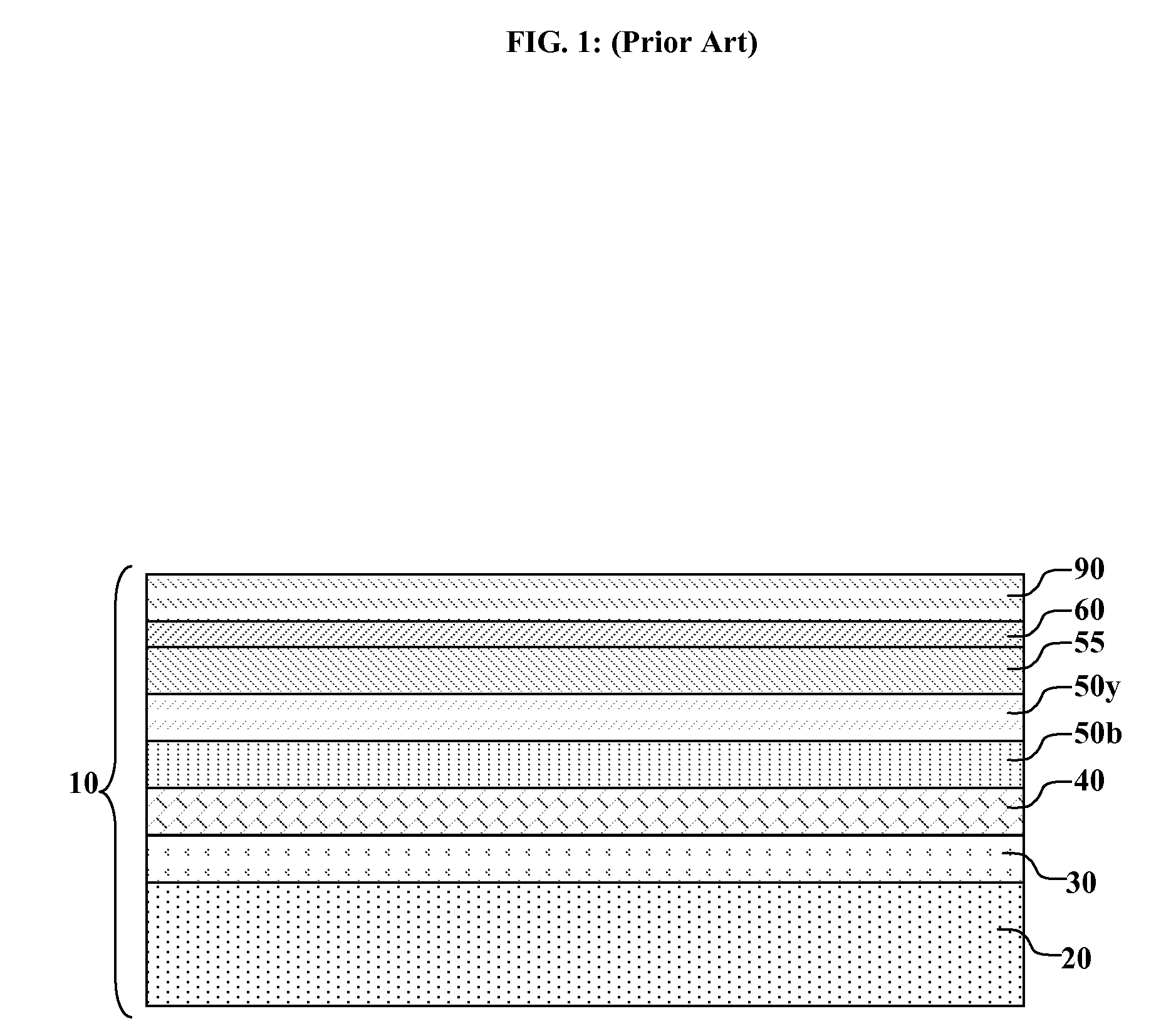
[0137]As shown in Table 1, the voltage rise for the inventive examples over the lifetime of the device was smaller than for the comparative device.

TABLE 1Device data measured at 20 mA / cm2 (except fade data)Room TempLumFade StabilityEfficienc...


PUM


Abstract

An inverted OLED device, comprising: a substrate; a cathode disposed on the substrate; an anode spaced from the cathode; at least one light-emitting layer disposed between the anode and the cathode; a hole-transporting layer disposed between the anode and the light-emitting layer(s); an electron-transporting layer disposed between the cathode and the light-emitting layer(s); a first electron-accepting layer disposed between the hole-transporting layer and the anode and including a first electron-deficient organic material constituting more than 50% by volume of the first electron-accepting layer and having a reduction potential greater than −0.5 V vs. a Saturated Calomel Electrode; and a second electron-accepting layer disposed between the electron-transporting layer and the cathode including a second electron-deficient organic material constituting more than 50% by volume of the second electron-accepting layer and having a reduction potential greater than −0.5 V vs. a Saturated Calomel Electrode.

Description

FIELD OF THE INVENTION[0001]The present invention relates to OLED devices, and in particular to inverted OLED devices.BACKGROUND OF THE INVENTION[0002]An organic light-emitting diode device, also called an OLED, commonly includes an anode, a cathode, and an organic electroluminescent (EL) unit sandwiched between the anode and the cathode. The organic EL unit includes at least a hole-transporting layer (HTL), a light-emitting layer (LEL), and an electron-transporting layer (ETL). OLEDs are attractive because of their low drive voltage, high luminance, wide viewing-angle, and capability for full color displays and for other applications. Tang et al. described this multilayer OLED in their U.S. Pat. Nos. 4,769,292 and 4,885,211.[0003]OLED devices are often constructed with the positive electrode or anode placed in contact with the substrate or support on which the OLED is constructed. This is known as normal or non-inverted OLED configuration. Low power consumption displays typically u...

Claims


Application Information

Patent Timeline
Patent Type & Authority Applications(United States)
IPC IPC(8): H01L27/28H01J9/02
CPCH01L51/0072H01L2251/554H01L51/5092H01L51/5088H10K85/6572H10K50/17H10K50/171H10K2101/50H10K71/00
Inventor SPINDLER, JEFFREY P.HATWAR, TUKARAM K.
Owner GLOBAL OLED TECH
Why Eureka
Try Eureka