Semiconductor device with sti and method for manufacturing the semiconductor device

a semiconductor and semiconductor technology, applied in the direction of semiconductor devices, electrical devices, transistors, etc., can solve the problems of difficult etching of polysilicon layers, difficulty increases, and impede the improvement of integration density, so as to reduce the height difference and increase the margin of photolithography process

Active Publication Date: 2009-04-23
FUJITSU LTD
View PDF14 Cites 21 Cited by
  • Summary
  • Abstract
  • Description
  • Claims
  • Application Information

AI Technical Summary

Benefits of technology

[0044]A height difference can be reduced and a margin of a photolithography process can be increased.

Problems solved by technology

An isolation region made by local oxidation of silicon (LOCOS) produces bird's beak portion which gradually reduces its thickness from a target silicon oxide film thickness, narrows an active region area and constitutes wasteful area, hindering improvement of an integration density.
It is not always easy to etch the polysilicon layer whose surface is covered with the ONO film.
This difficulty increases if the peripheral area of the active region is surrounded by STI having a concave portion or a protrusion portion and etching is performed at a sloped surface.
A semiconductor device integrating a flash memory area and a logic circuit area may have a problem different from the problem of a semiconductor device integrating a DRAM memory cell area and a logic circuit area.

Method used


Image

  • Semiconductor device with sti and method for manufacturing the semiconductor device
  • Semiconductor device with sti and method for manufacturing the semiconductor device
  • Semiconductor device with sti and method for manufacturing the semiconductor device

Examples


first embodiment

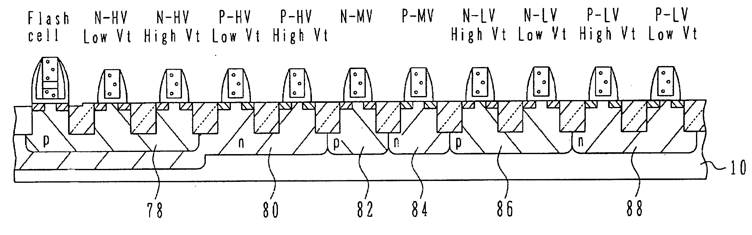
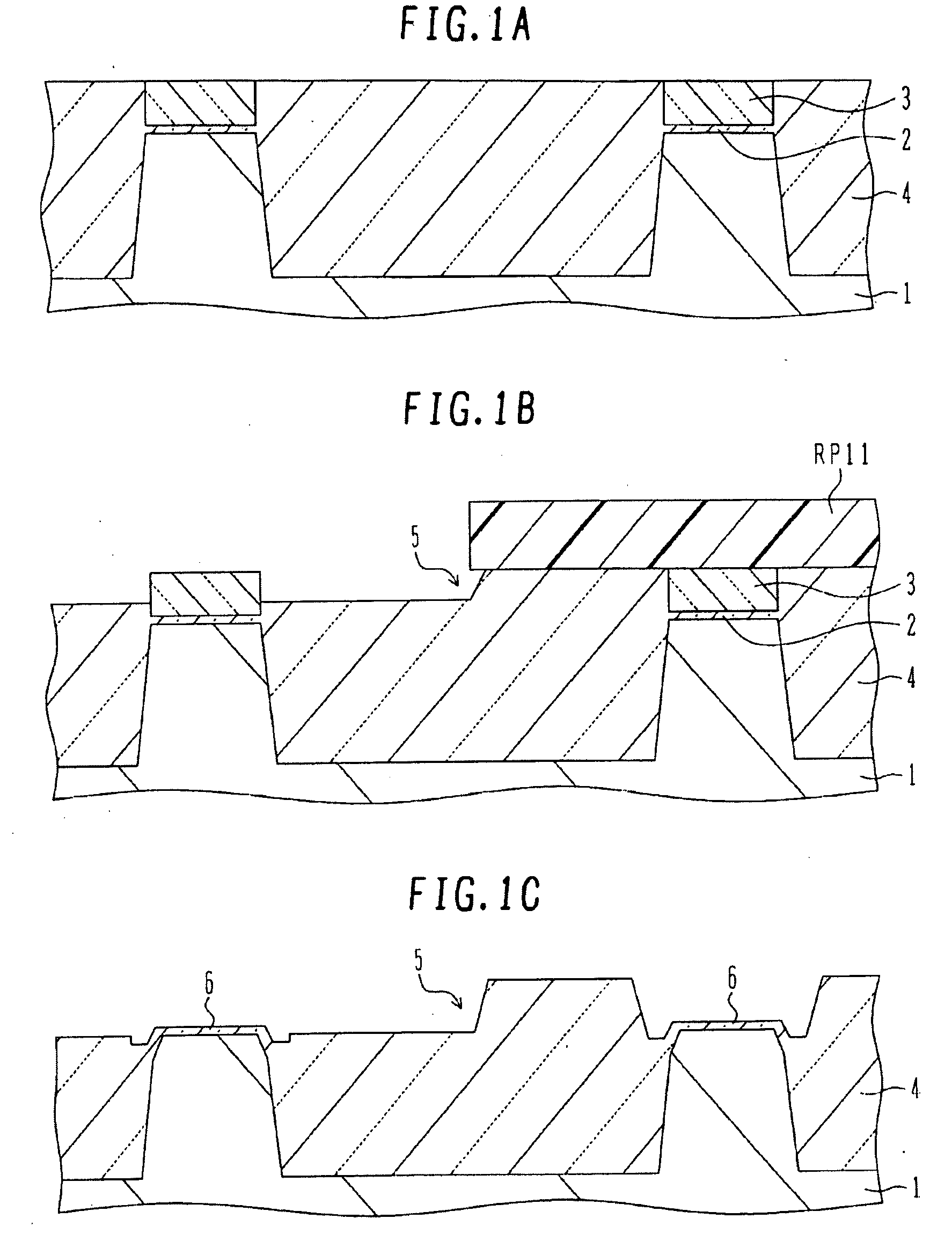
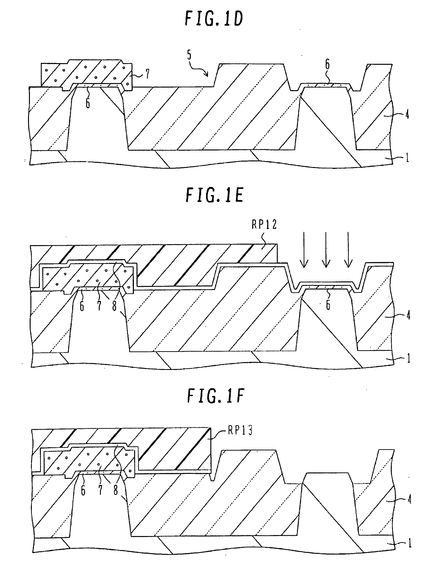
[0062]With reference to FIGS. 1A to 1K, description will be made on a method for manufacturing the semiconductor device according to the FIGS. 1A to 1I are cross sectional views illustrating main manufacture processes, FIG. 1J is a plan view showing the shapes of gate electrodes, and FIG. 1K is a cross sectional view of an area between control gates.

[0063]As shown in FIG. 1A, the surface of a silicon substrate 1 is thermally oxidized to form a buffer silicon oxide film 2 having a thickness of, e.g., 10 nm, and a silicon nitride film 3 having a thickness of, e.g., 110 nm is deposited on the silicon oxide film by CVD. By using a resist pattern, the silicon nitride film 3 and silicon oxide film 2 are patterned to leave a mask insulating film pattern made of a lamination of the buffer silicon oxide film 2 and silicon nitride film 3 and having a shape covering the active region. By using the silicon nitride film 3 as an etching mask, the silicon substrate is etched to a depth of, e.g., ...

third embodiment

[0083]A mask for partial etching of STI in the flash memory area may be used commonly as a mask for another process. With reference to FIGS. 3A and 3B, description will be made on a method for manufacturing a semiconductor device according to the

[0084]FIG. 3A is similar to FIG. 1A. The surface of a silicon substrate 1 is thermally oxidized to form a buffer silicon oxide film 2, and a silicon nitride film 3 is deposited on the silicon oxide film by CVD. By using a resist pattern, the silicon nitride film 3 and silicon oxide film 2 are patterned, and by using the silicon nitride film 3 as an etching mask, the silicon substrate is etched to form an isolation trench. A silicon oxide film 4 is deposited by HDPCVD to bury the isolation trench. CMP is performed starting from the surface of the silicon oxide film 4 to remove the silicon oxide film 4 above the surface level of the silicon nitride film 3.

[0085]As shown in FIG. 3B, a resist pattern RP31 for exposing the flash memory area is fo...


PUM


Abstract

A semiconductor device includes: a semiconductor substrate having first and second areas; an STI isolation region being made of an isolation trench formed in the semiconductor substrate and an insulating film burying the isolation trench and defining a plurality of active regions in the first and second areas; a first structure formed on an area from the active region in the first area to a nearby STI isolation region and having a first height; and a second structure formed on an area from the active region in the second area to a nearby STI isolation region and having a second height, wherein the surface of the said STI isolation region in the first area is lower than the surface of said STI isolation region in the second area.

Description

CROSS REFERENCE TO RELATED APPLICATION[0001]This application is based on PCT / JP2006 / 313083, filed on Jun. 30, 2006, the entire contents of which are incorporated herein by reference.BACKGROUND[0002]A) Field[0003]The embodiments relate to a semiconductor device with STI and a method for manufacturing the semiconductor device, and more particularly to a semiconductor device with STI having structures of different heights on a plurality of active regions, and a method for manufacturing the semiconductor device of this type. A semiconductor device has typically nonvolatile memory cells with floating gates and MOS transistors of logic circuits.[0004]B) Description of the Related Art[0005]In a semiconductor integrated circuit device (IC), a logic circuit is usually made of a complementary MOS (CMOS) circuit including n-channel MOS (NMOS) transistors and p-channel MOS (PMOS) transistors in order to reduce consumption power. In order to meet the requirements for high integration and high sp...

Claims


Application Information

Patent Timeline
Patent Type & Authority Applications(United States)
IPC IPC(8): H01L29/06H01L21/762
CPCH01L21/76232H01L27/105H01L27/11526H01L27/11536H01L27/11546H01L29/788H01L27/11575H01L29/42336H01L29/7881H01L21/762H01L27/11548H10B41/40H10B41/44H10B41/49H10B41/50H10B43/50
Inventor EMA, TAIJIMIZUTANI, KAZUHIRO
Owner FUJITSU LTD
Why Eureka
Try Eureka