

Track-And-Hold Circuit With Adjustable Charge Compensation
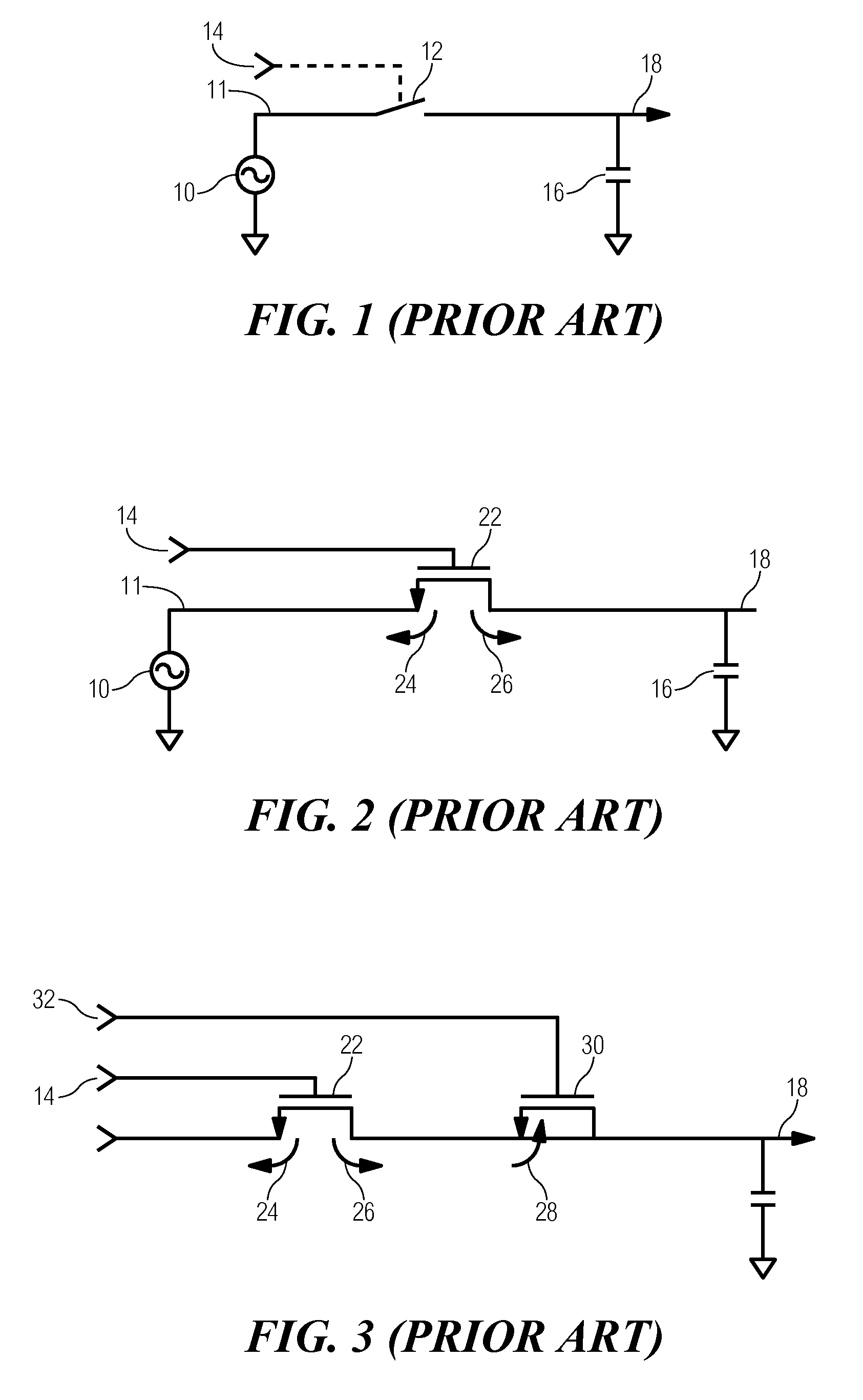
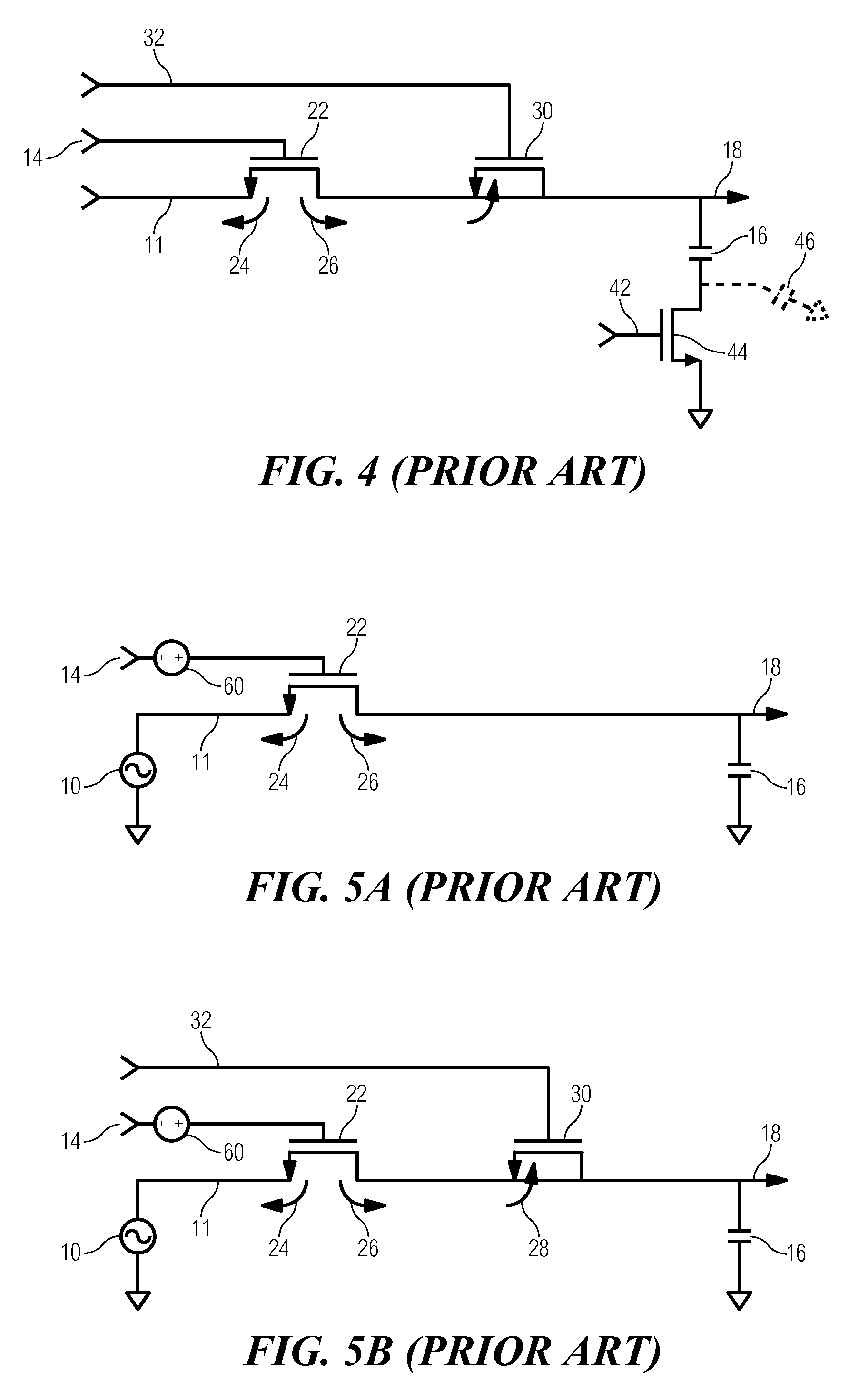
a track and hold circuit technology, applied in the field of track hold circuits with adjustable charge compensation, can solve the problems of difficult implementation of prior art in practice, significant performance issues, and unsatisfactory t/h circuits shown in fig. 1 and fig. 2
- Summary
- Abstract
- Description
- Claims
- Application Information
AI Technical Summary
Problems solved by technology
Method used
Image

Examples
second embodiment
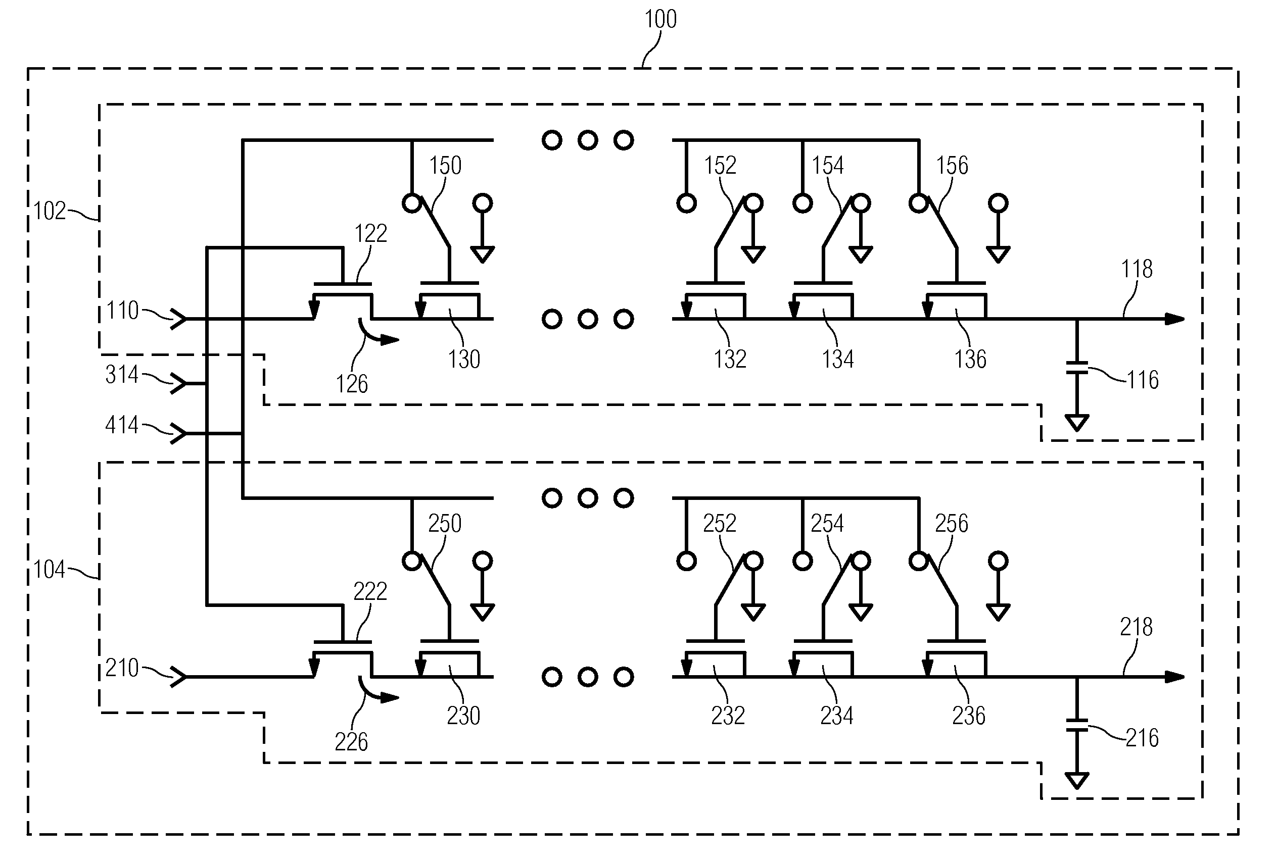
[0044]FIG. 6B is a diagram of the inventive T / H circuit in a single-ended mode. The embodiment of FIG. 6B is similar to that of top half 102 in FIG. 6A and includes a device 161 to create a pseudorandom sequence and a control device 162 to select charge compensation devices 130-136 to operate within or out of the T / H circuit (described in detail below).
[0045]Device 161 is a pseudorandom number generator or a noise-shaping modulator, such as a delta-sigma modulator. For example, a pseudorandom number generator (PRNG) would supply a new pseudorandom number (PRN) for every track-and-hold cycle. The PRN determines which combination of charge compensation devices to use in a particular T / H cycle (also referred to as a sample) and provides a different PRN on a sample-by-sample basis.
[0046]When compensating charge injection 126 by charge compensation devices 130-136 in a random manner, the pedestal voltage at output node 118 is statistically uncorrelated to the input voltage 110. The pedes...
third embodiment
[0050]Charge compensation devices can be incorporated into bottom-plate sampled and bootstrapped T / H circuits. FIG. 7 is a schematic diagram of the invention incorporating bottom-plate sampling. The circuit in FIG. 7 is similar to that shown in FIG. 6A and has two additional NMOS switches 144 and 244 connected to the bottom-plate of capacitors 116 and 216 respectively. The control terminals of switches 144 and 244 are connected to Sample 342.
[0051]In the circuit described in FIG. 7, Sample 342 is brought low prior to Clock 314 going low. This open-circuits the bottom-plate of capacitors 116 and 216, defining the sampling instant. With the bottom-plate of both capacitors open-circuited, the charge stored on the capacitors ideally remains constant, regardless of the voltage fluctuation on the output voltage node 118 or 218. With Sample held low, Clock 314 is then brought low (hold phase). Clock 414 is brought high, forcing injected charge 126 or 226 to be partially compensated by the ...
fourth embodiment
[0056]FIG. 8 is a schematic diagram of the invention incorporating bottom-plate sampling as well as a bootstrap voltage supply.
[0057]The circuit in FIG. 8 is similar to that in FIG. 7 and has an additional voltage source in each half (102 and 104) of the T / H circuit 100. In top half 102, voltage source 160 is located between the control terminal of the tracking switch 122 and Clock 314. The voltage at source 160 is set to track the input voltage source 110.
[0058]Similarly, a voltage source 260 is located between the control terminal of the tracking switches 222 and Clock 314. The voltage at source 260 is set to track the input voltage source 210.
[0059]Incorporating a bootstrapped voltage source in T / H circuit 100 as shown in FIG. 8, helps maintain a constant voltage differential at the gate and source (Vgs) terminals of tracking switches 122 and 222 at every Clock 314 cycle.
[0060]A constant Vgs on tracking switches 122 and 222 during the track phase improves the linearity of the swi...
PUM
 Abstract
Description
Claims
Application Information