
Filament lamp and heat treatment device of the light irradiation type

a heat treatment device and light irradiation technology, applied in lighting and heating apparatus, drying, furnaces, etc., can solve the problems of defective items, defects in crystal transition, and slipping of semiconductor wafers, so as to increase the electrical resistance of filaments, increase the surface area of filaments, and increase the length of bare wires

Inactive Publication Date: 2009-04-23
USHIO DENKI KK
View PDF2 Cites 10 Cited by
  • Summary
  • Abstract
  • Description
  • Claims
  • Application Information

AI Technical Summary

Benefits of technology

[0029]Here, using bundled wires and adjusting the number of bare wires, the electrical resistance of the filaments can be adjusted to nearly any level, so that problems like the filaments becoming too thick and coming into contact with the light-emitting tube or the rigidity of the filament falling to the point that the coils cannot be held in place can be avoided and the desired power density can be engineered.
[0030]Also, with this invention, by twisting the bundled wires into twisted wires, it is possible to increase the length of the bare wires per unit of filament length in comparison with the bare wires that are simply bundled together, making it possible to increase the electrical resistance of the filament and raise the power density, broadening the freedom of design to allow the accommodation of a variety of article to be treated. Furthermore, the rigidity of the filaments can be improved by using fine, bare wires, which makes it possible to avoid the problem of filaments deforming under their own weight. Also, when five or more bundled wires are used, the peripheral area increases in opposition to the other bundled wires and the surface area grows smaller with respect to the weight per unit of filament length. For this reason, using two to four bundled wires makes it possible to avoid increases to an undesired length while increasing the surface area very efficiently while avoiding an undesired decline in electrical resistance while preventing deformation of the filament under its own weight.
[0031]Furthermore, by having the same color temperature for the light that is emitted from each of the filaments arranged around the peripheral edge zone of the article to be treated and each of the filaments arranged around the center zone of the article to be treated (in other words, having the surface temperature of the filaments be the same), it is possible to make the spectra of the light that is radiated to the article to be treated identical, and to make the light absorption over the entire area of the article to be treated uniform.
[0032]Additionally, by using a heat treatment device of the light irradiation type in which multiple filament lamps have been arranged in parallel, it is possible to achieve rapid and uniform heating of the article to be treated.

Problems solved by technology

At the same time, when heat-treating a semiconductor wafer (silicon wafer) to 1050° C. or higher, when there is non-uniform distribution of heat on the semiconductor wafer, the semiconductor wafer will undergo a phenomenon known as “slip.” In other words, there would be a risk of defects in the crystal transition, leading to defective items.
However, even when using the filament lamp 100 that has multiple filaments with independent power supplies like the one shown in FIG. 11, there are times when the uniform heating of a semiconductor wafer or other article to be treated is impossible.
This would cause a temperature difference to occur between the center area and the peripheral edge of the article to be treated, making it impossible to heat the article uniformly.

Method used


Image

  • Filament lamp and heat treatment device of the light irradiation type
  • Filament lamp and heat treatment device of the light irradiation type
  • Filament lamp and heat treatment device of the light irradiation type

Examples


Embodiment Construction

[0046]An embodiment of the present invention will now be explained using FIGS. 1 through 10.

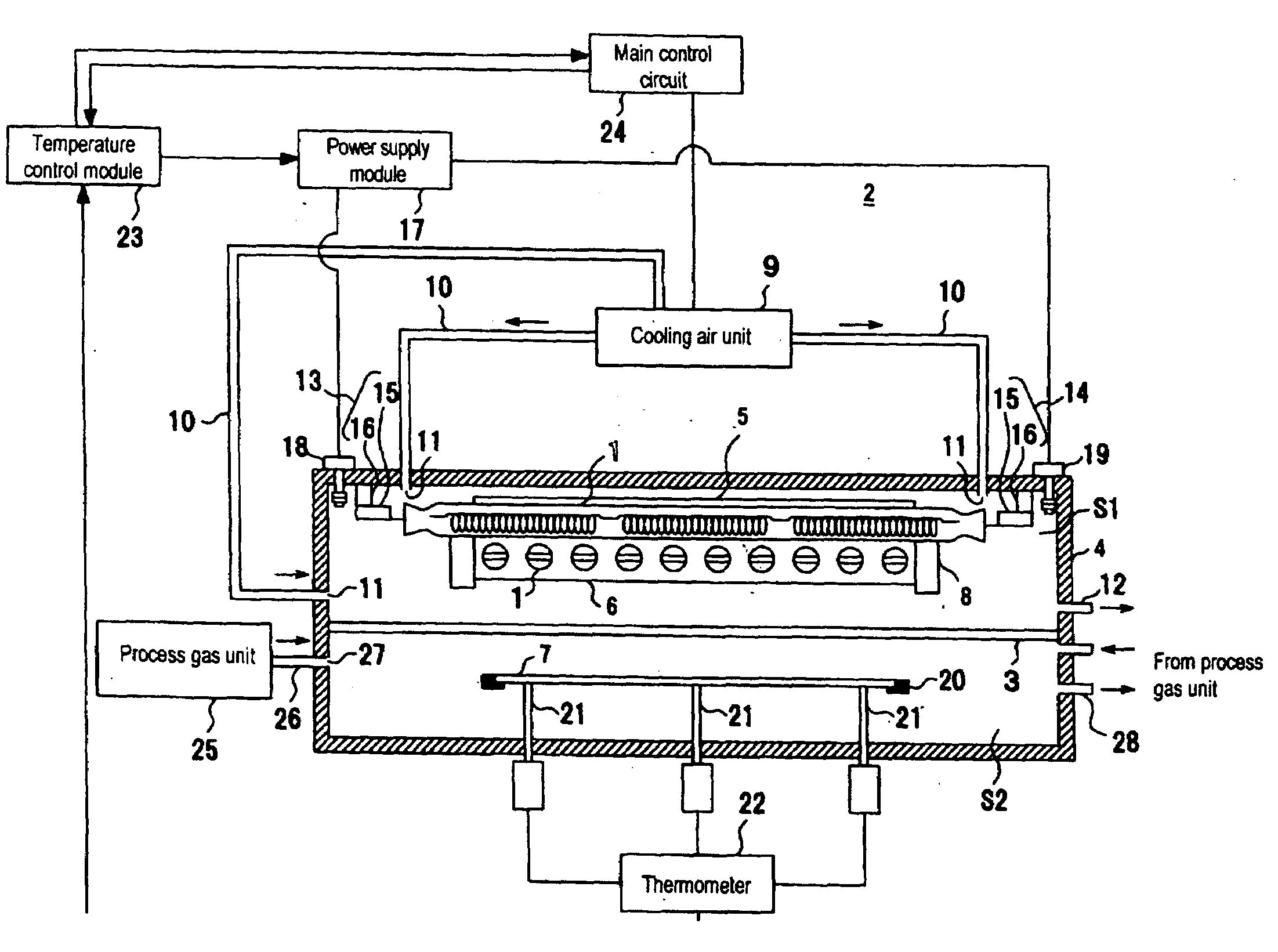
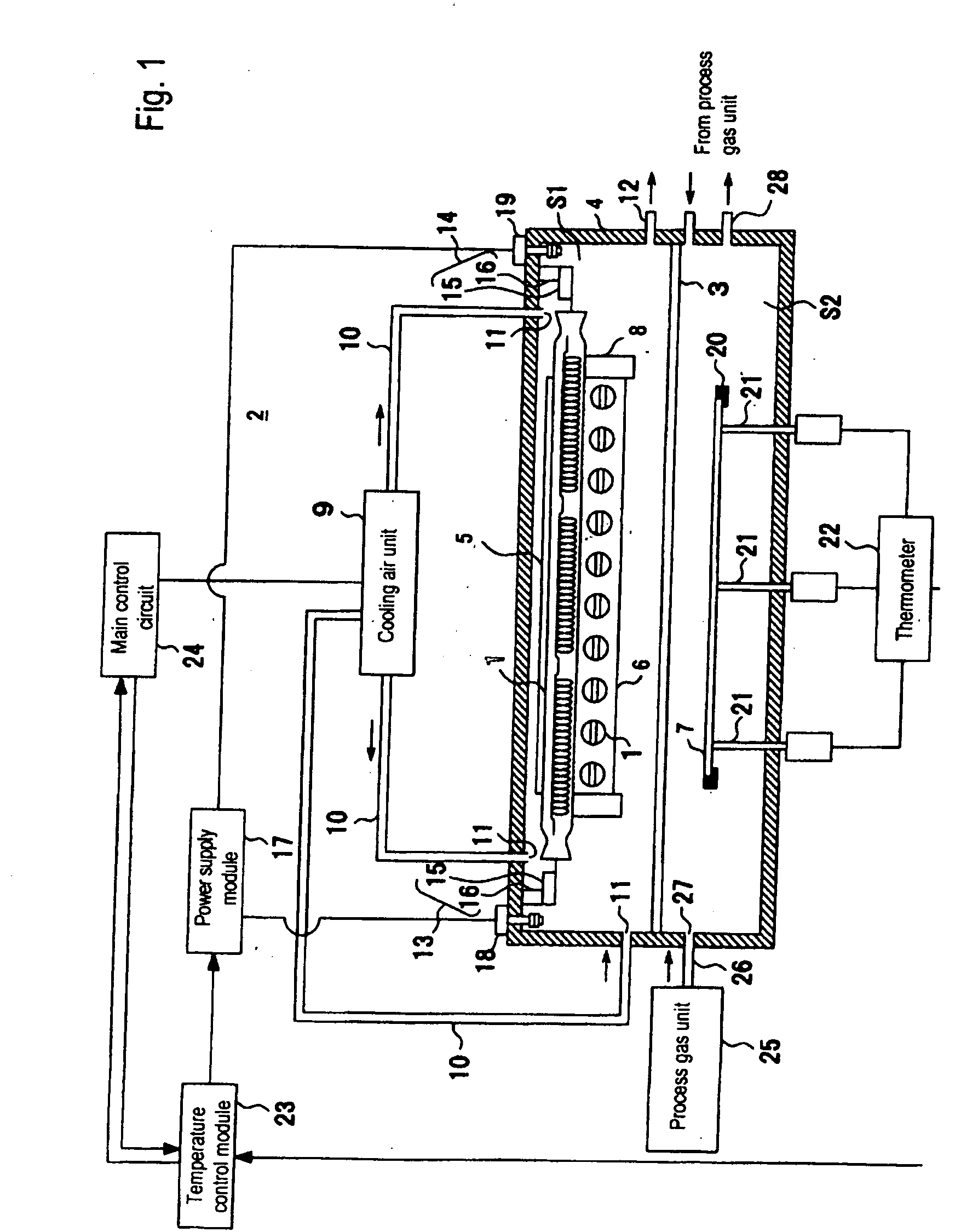
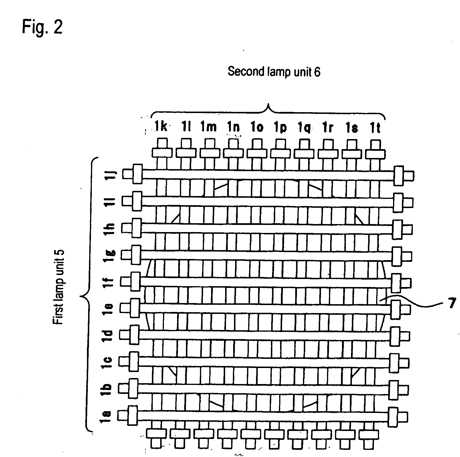
[0047]FIG. 1 is a cross-section diagram of a heat treatment device of the light irradiation type according to an embodiment of the invention, configured with multiple filament lamps that have independent power supplies and are arranged in parallel. FIG. 2 is a diagram of the article to be treated looking at it from above the heat treatment device of the light irradiation type shown in FIG. 1, through the multiple filament lamps arranged in parallel.

[0048]As shown in FIG. 1, this heat treatment device of the light irradiation type 2 has a chamber that is divided into a lamp unit housing space S1 and a heat-treatment space S2 using a transparent quartz window 2, a quartz glass window for example. The light emitted from the first lamp unit 5 and the second lamp unit 6 that are arranged in the lamp unit housing space S1 passes through the quartz window 3 and performs the heat treatment of the art...


PUM


Abstract

Filament lamps whose individual filament coils can be set to specific temperatures in filament lamps that are supplied with electric power independently and to provide a heat treatment device of the light irradiation type that uses said lamps. Inside of a light emitting tube of each lamp, which has the hermetically sealed portions at each end, are multiple filament modules which have been made by linking pairs of leads which supply electrical power to both ends of coiled filaments and individual filaments that are placed so that they extend along the axis of the light emitting tube. In the electrically connected filament lamps, whose individual leads are connected to the respective electrically conductive material placed in the hermetically sealed portions, at least one of the individual filaments is made up of a single wire and at least two are made up of bundled wires with the single wire being located between the bundled wires.

Description

BACKGROUND OF THE INVENTION[0001]1. Field of Invention[0002]The present invention pertains to heat treatment devices of the light irradiation type in which filament lamps are supplied with electrical power independently and many such filament lamps are arranged in parallel.[0003]2. Description of Related Art[0004]Generally, in semiconductor manufacturing processes, a silicon oxide film is formed, and by means of a wide variety of processes, including the diffusion of impurities, requiring rapid heat treatments or the uniform heating of an article to be treated.[0005]Japanese Unexamined Patent Application Publication 2006-279008 and corresponding U.S. Patent Application Publication 2006 / 197454 describe a heat treatment device of the light irradiation type that is configured as follows. In order to heat an article to be treated by light emitted from filaments, multiple filament lamps are equipped with coiled filaments having differing overall lengths that are arranged in individual li...

Claims


Application Information

Patent Timeline
IPC IPC(8): F26B3/30H01K7/00
CPCH01K1/14H01L21/67115H01K9/00H01K1/16
Inventor TANINO, KENJIMIZUKAWA, YOICHISUZUKI, SHINJI
Owner USHIO DENKI KK
Learn More