

Transistor and method of fabricating the same
a technology of transistors and transistors, applied in the field of transistors, can solve the problems of reducing the mobility of carriers, generating stacking faults in interfaces, and deteriorating performance of transistors, so as to prevent the increase of resistance and stacking faults, and improve the performan
- Summary
- Abstract
- Description
- Claims
- Application Information
AI Technical Summary
Benefits of technology
Problems solved by technology
Method used
Image

Examples
first embodiment
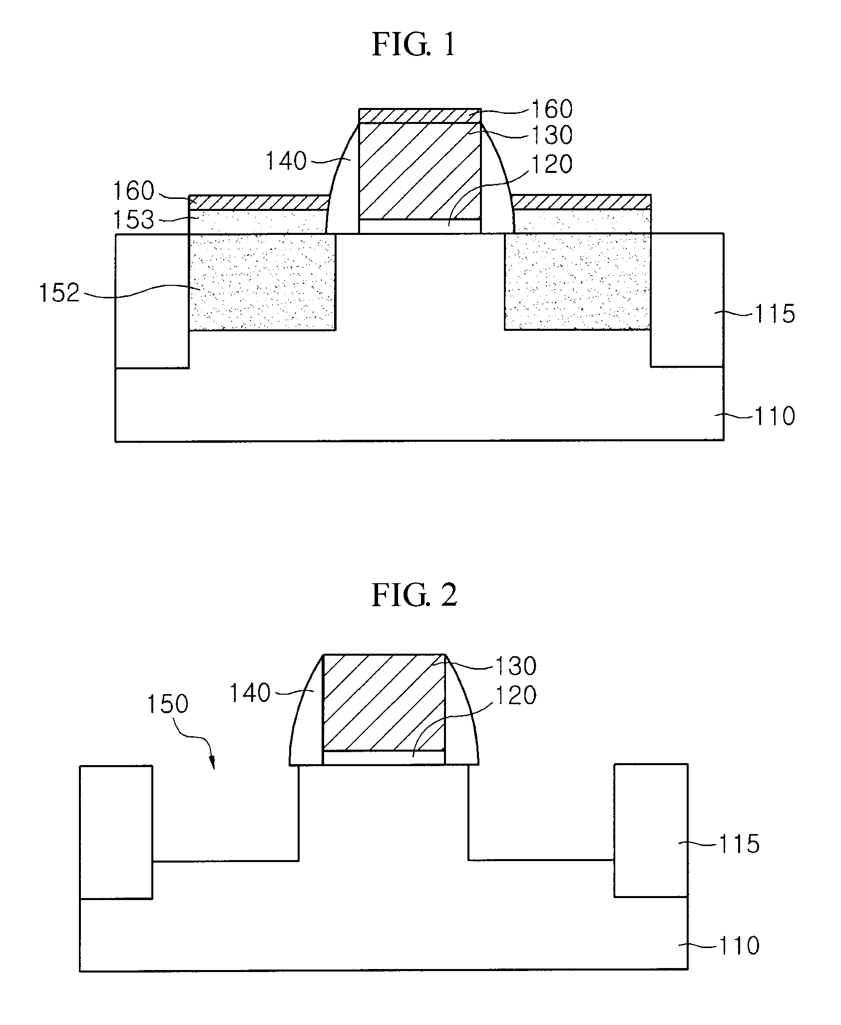
[0035]FIG. 1 illustrates a cross-sectional view of a transistor in accordance with the present invention.
[0036]Referring to FIG. 1, the transistor includes a gate insulation layer 120 and a gate electrode 130 that are formed in a stack structure on a substrate 110, a spacer 140 formed on sidewalls of the gate electrode 130, an epitaxial layer 152 formed in a recess region of the substrate 110 at both sides of the gate electrode 130 and acting as source and drain regions, a capping layer 153 formed on the epitaxial layer 152, and a silicide layer 160 formed on the gate electrode 130 and the capping layer 153. Herein, the epitaxial layer 152 and the capping layer 153 are formed of SiGe and the concentration of Ge contained in the capping layer 153 is lower than that of Ge contained in the epitaxial layer 152. Furthermore, the concentration of Ge contained in the capping layer 153 may be gradually reduced as going from a lower portion to an upper portion. In accordance with another emb...
second embodiment
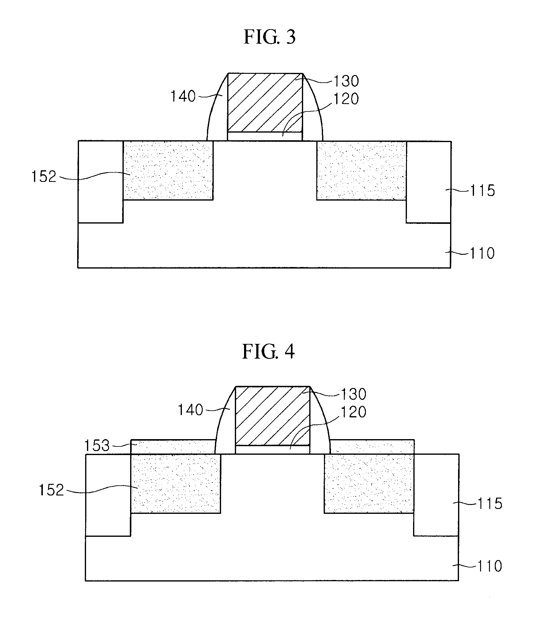
[0050]FIG. 6 illustrates a cross-sectional view of a transistor in accordance with the present invention. By forming a seed layer including a SiGe layer that contains Ge having the concentration in a range of approximately 5% to approximately 15% before forming an epitaxial layer, it is possible to remove a stacking fault being apt to occur at a lower portion of a recess region due to the epitaxial layer containing Ge whose concentration is greater than 25%. The increase of resistance is prevented by forming a capping layer.
[0051]Referring to FIG. 6, the transistor in accordance with the second embodiment of the present invention includes a gate insulation layer 120 and a gate electrode 130 that are formed in a stack structure on a substrate 110, a spacer 140 formed on sidewalls of the gate electrode 130, a seed layer 151 and an epitaxial layer 152 formed in a recess region of the substrate 110 at both sides of the gate electrode 130, a capping layer 153 formed on the epitaxial laye...
third embodiment
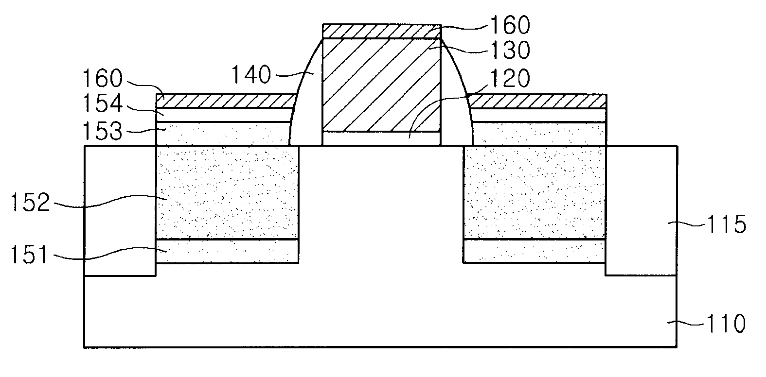
[0056]FIG. 7 illustrates a cross-sectional view of a transistor in accordance with the present invention.
[0057]Referring to FIG. 7, the transistor includes a gate insulation layer 120 and a gate electrode 130 that are formed in a stack structure on a substrate 110, a spacer 140 formed on sidewalls of the gate electrode 130, a seed layer 151 and an epitaxial layer 152 formed in a recess region of the substrate 110 at both sides of the gate electrode 130, a first and a second capping layer 153 and 154 formed on the epitaxial layer 152, and a silicide layer 160 formed on the gate electrode 130 and the second capping layer 154. Herein, the seed layer 151, the epitaxial layer 152 and the first capping layer 153 are formed of SiGe and the concentration of Ge contained in the seed layer 151 and the first capping layer 153 is lower than that of Ge contained in the epitaxial layer 152. Furthermore, the concentration of Ge contained in the first capping layer 153 may be gradually reduced as g...
PUM
 Abstract
Description
Claims
Application Information