Semiconductor integrated circuit device

Inactive Publication Date: 2009-04-30
HITACHI LTD
View PDF8 Cites 11 Cited by
  • Summary
  • Abstract
  • Description
  • Claims
  • Application Information

AI Technical Summary

Benefits of technology

[0008]In a test employing a scan test, when an entire chip is driven by one test clock distributed from the origin of the clock tree, since random numbers are input from the scan chains to all the scan flip-flops driven by the test clock, the activation rate of the entire chip is instantaneously increased significantly higher than that of a normal usage state. As a result, there is a possibility that unexpected voltage drop of the power supply and power supply noise occur, the scan flip-flops malfunction, and correct test results cannot be obtained. Further, the clock in the scan test can be subjected to time sharing for each region in order to reduce the power supply noise. In this case, however, scan chains which are present across the time-shared clock regions are generated. Whe

Problems solved by technology

As a result, there is a possibility that unexpected voltage drop of the power supply and power supply noise occur, the scan flip-flops malfunctio

Method used


Image

  • Semiconductor integrated circuit device
  • Semiconductor integrated circuit device
  • Semiconductor integrated circuit device

Examples


Embodiment Construction

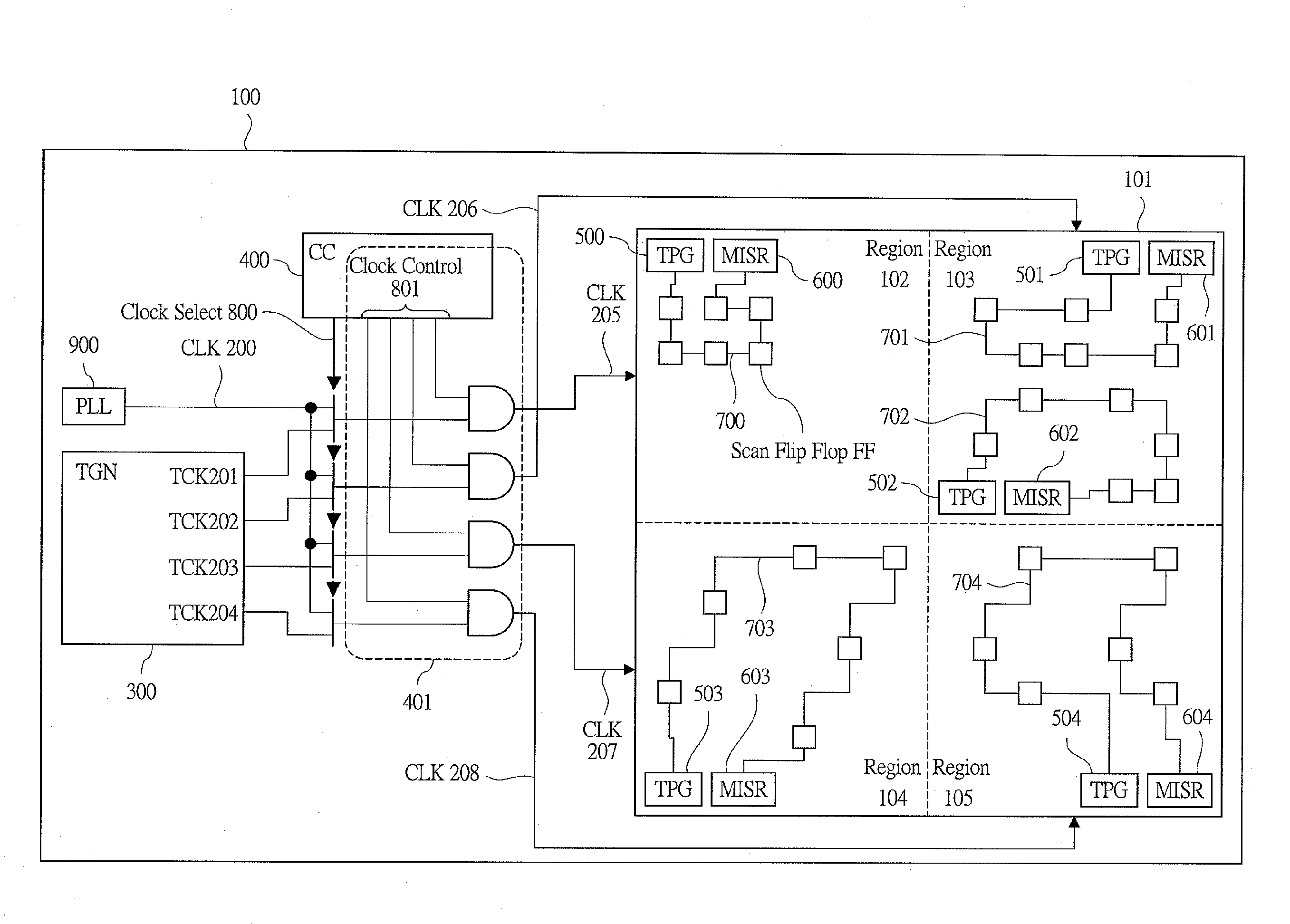
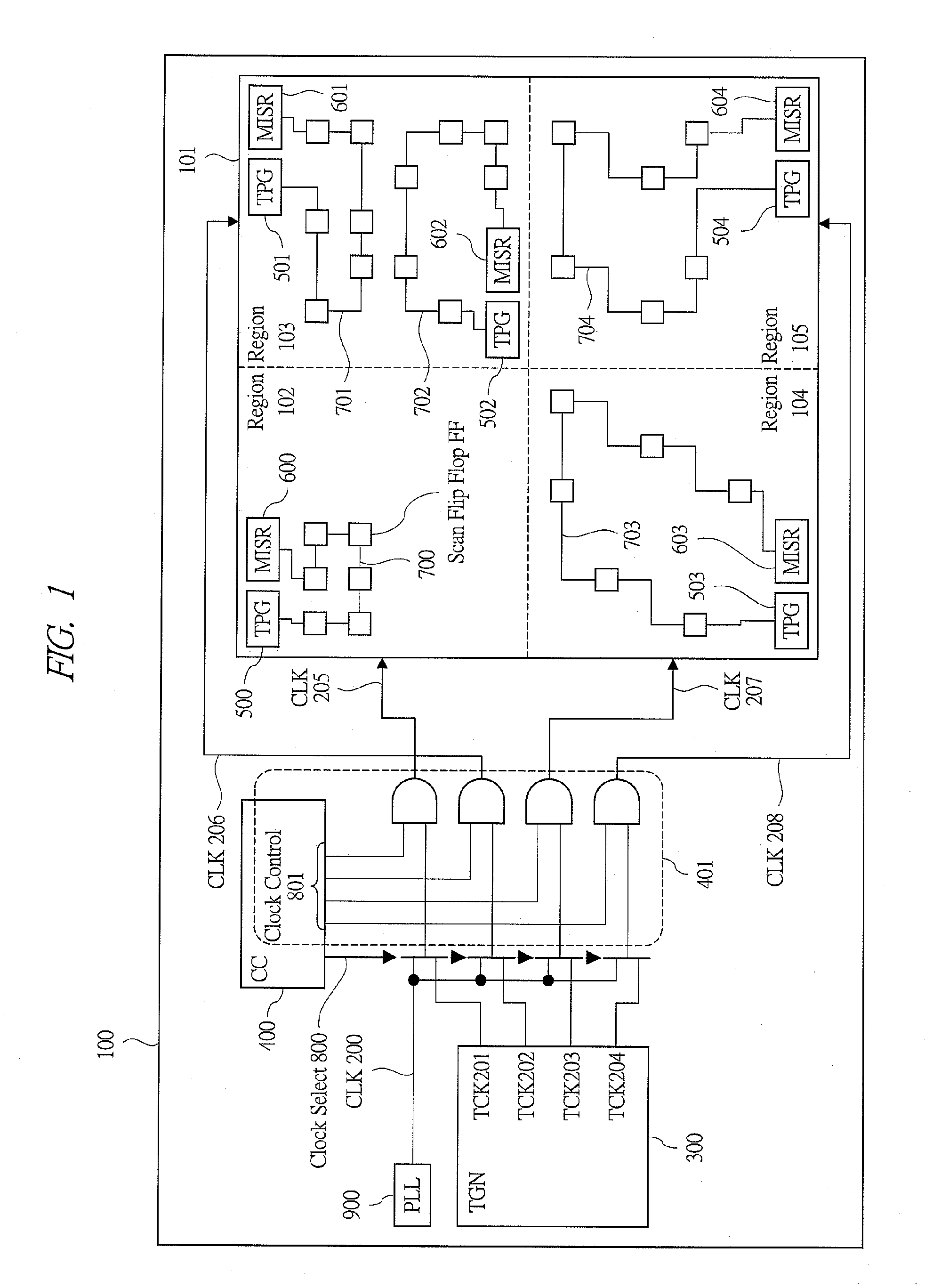
[0023]Hereinafter, a circuit configuration will be described with reference to FIGS. 1, 3 and 4, a test method will be described with reference to FIGS. 5 to 7, and a circuit designing method will be described with reference to FIGS. 8 and 10.

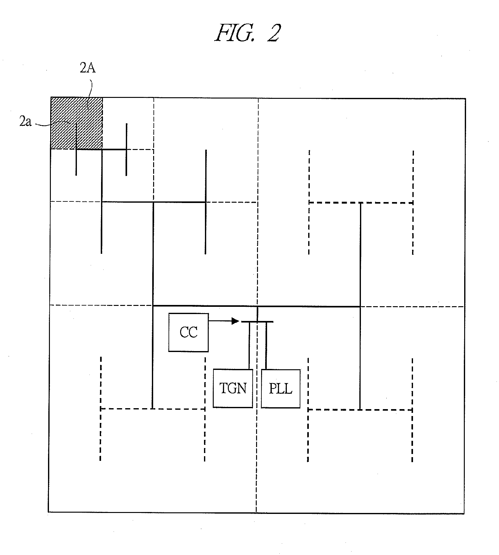
[0024]First, the circuit configuration will be described with reference to FIGS. 1, 3 and 4. FIG. 1 is a drawing showing the idea of the entire configuration of a scan noise prevention post-layout reorder method according to an embodiment of the present invention. In FIG. 1, 100 denotes the entirety of a semiconductor integrated circuit device, 101 denotes a circuit part to be inspected which is a scan target, 200 denotes a normal clock CLK, 300 denotes a test clock generator TGN which generates test clocks to be input in scan-in / out or a static test, 400 denotes a clock controller CC which controls switching of the clocks input to a test circuit and on / off of the input, 500 to 504 denote test pattern generators TPG which generate test patterns...


PUM


Abstract

A scan chain group structure in which a group of scan chains formed for each clock tree system in an LSI is subjected to a reconnection process so that the scan chain group is not present across a plurality of clock distribution regions obtained by dividing the clock-supplied region of the clock tree of one system and that the connection distance thereof in the distribution region becomes short, a test clock input mechanism in which test clocks to be input to the distribution regions are independent sub-clock phases, and an on/off mechanism of the clocks to be input to the distribution regions are realized. Further, the scan-in/out and scan test performed at the same time are limited in one region or between single regions, and tests in all regions and between all regions are carried out by a plurality of times of test steps.

Description

CROSS-REFERENCE TO RELATED APPLICATION[0001]The present application claims priority from Japanese Patent Application No. JP 2007-278308 filed on Oct. 26, 2007, the content of which is hereby incorporated by reference into this application.TECHNICAL FIELD OF THE INVENTION[0002]The present invention relates to a semiconductor integrated circuit device. More particularly, it relates to the reduction of noise caused by power supply voltage drop in a test of a semiconductor integrated circuit device.BACKGROUND OF THE INVENTION[0003]Conventional techniques related to a test of a semiconductor integrated circuit include the technique described in Japanese Patent Application Laid-Open Publication No. 2003-240822 (Patent Document 1). In the method of Patent Document 1, the duties of the clocks input to scan chains which are respectively formed for clock systems are changed so that the number of flip-flops operated at the same time is reduced, thereby reducing power-supply noise. In the conve...

Claims


Application Information

Patent Timeline
IPC IPC(8): G01R31/3183G06F11/263G06F1/10H01L21/8232
CPCG01R31/318552
Inventor ITO, YUICHIFUJIMURA, YASUHIROTSUTSUMIDA, KOKINAKAHARA, SHIGERU
Owner HITACHI LTD
Why Eureka
Try Eureka