Pulse operated flip-flop circuit having test-input function and associated method

a flip-flop circuit and input function technology, applied in the field of pulse-operated flip-flop circuits having input functions, can solve the problems of increasing the delay in outputting data, adding further limitations to scan tests, and flip-flops capable of operating at high speed, so as to reduce the length of data transfer paths, reduce the dtoq delay, and high speed

Active Publication Date: 2009-05-07
SAMSUNG ELECTRONICS CO LTD
View PDF2 Cites 16 Cited by
  • Summary
  • Abstract
  • Description
  • Claims
  • Application Information

AI Technical Summary

Benefits of technology

[0036]Accordingly, in accordance with the flip-flop circuits and the method of latching data, the length of data transfer path is reduced, thereby decreasing the DtoQ delay, even though the test-input function is implemented. Thus the latched data may be output at a relatively high speed. Also area occupied by the flip-flop circuit integrated on a chip may be reduced according to contraction of the data transfer path.

Problems solved by technology

As semiconductor integrated circuits become complicated, further limitations are added to the scan test and flip-flops capable of operating at high speed are required.
The conventional flip-flop circuit 100 sequentially transfers data during each two cycles of the clock signal CK, thereby increasing delay in outputting data.
The master-slave flip-flops having such configurations are inadequate for high-speed semiconductor devices due to relatively large DtoQ delay between input and output of the flip-flop.

Method used


Image

  • Pulse operated flip-flop circuit having test-input function and associated method
  • Pulse operated flip-flop circuit having test-input function and associated method
  • Pulse operated flip-flop circuit having test-input function and associated method

Examples


Embodiment Construction

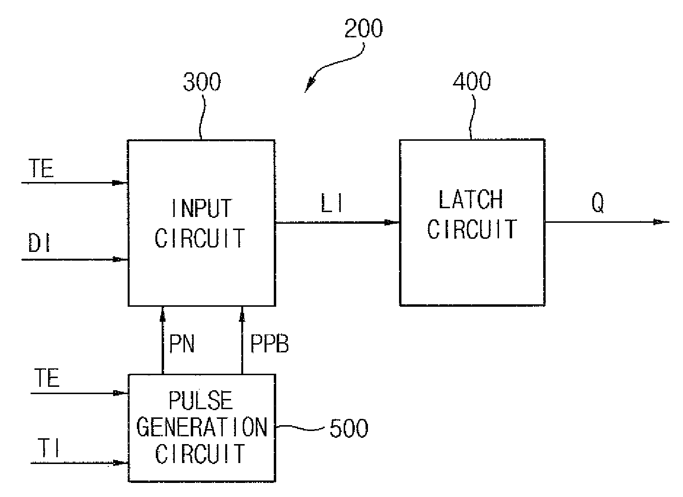
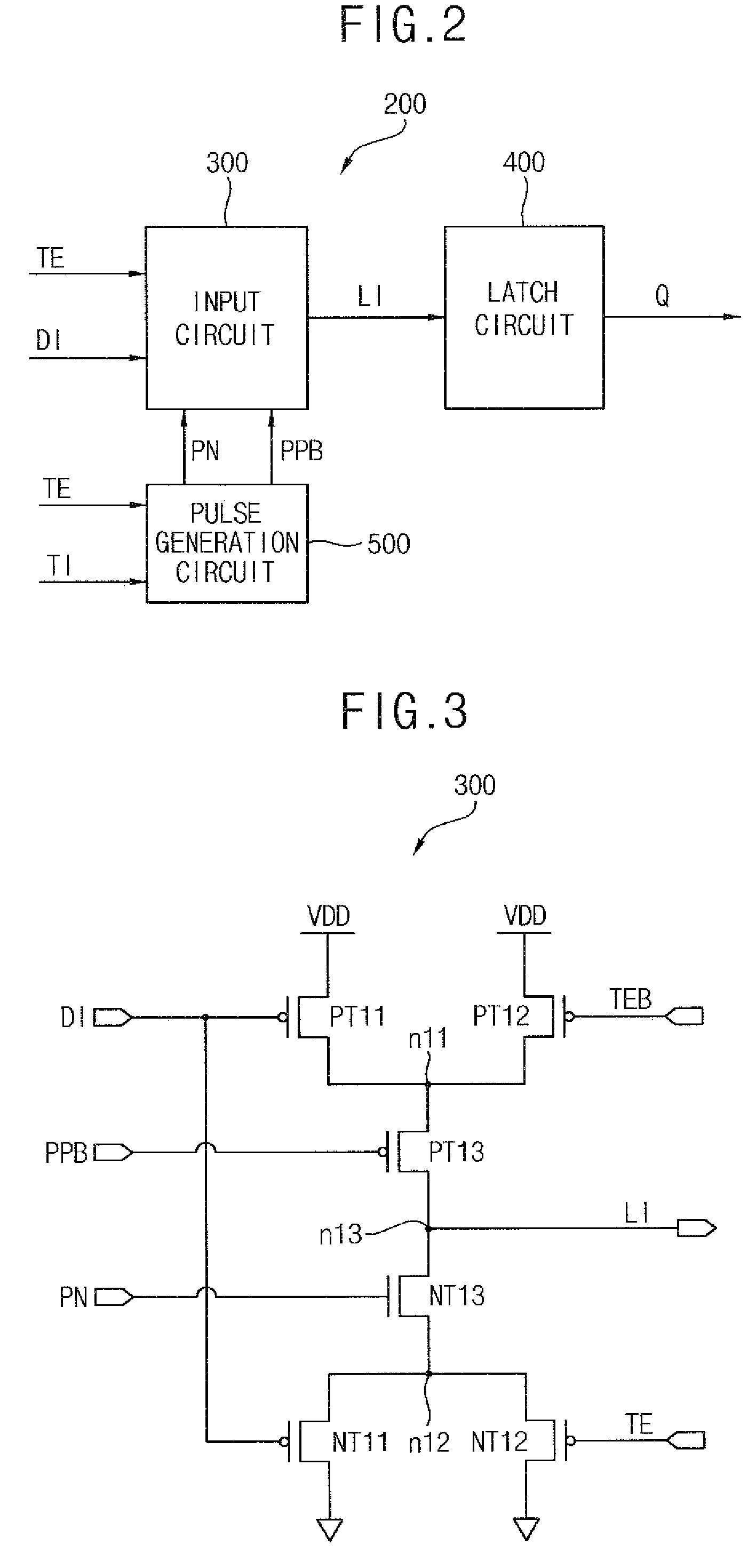
[0055]FIG. 2 is a block diagram of a flip-flop circuit having a test-input function according to an exemplary embodiment of the invention.

[0056]Referring to FIG. 2, a flip-flop circuit 200 includes an input multiplexing circuit 300 (see FIG. 3), a latching circuit 400 (e.g., the simple latches 400a or 400b of FIG. 4 and FIG. 5 or interruptible latches 400c, 400d, 400e, 400f of FIGS. 6, 7, 17 or 19, or a six-transistor SRAM memory cell) and a pulse generation circuit 500.

[0057]The pulse generation circuit 500 generates a first pulse signal PN and a second (complementary) pulse signal PPB such that the first and second pulse signals PN and PPB are activated simultaneously in a normal mode and activated selectively in response to a test input signal TI in a test mode. The input multiplexing circuit 300 selects and outputs one of the data input signal DI and the test input signal TI as a latch input signal LI in response to the first pulse signal PN and the second pulse signal PPB. The ...


PUM


Abstract

The pulse generation circuit generates a first pulse signal and a complementary second pulse signal. The first and second pulse signals are activated simultaneously in a normal mode and activated selectively in response to a test input signal in a test mode. A multiplexing input circuit selects and outputs one of a data input signal and a test input signal as a latch input signal in response to the first pulse signal and the second pulse signal. The latch input signal corresponds to the data input signal in the normal mode and corresponds to the test input signal in the test mode. The latching circuit latches the latch input signal to generate data output signal. The length of data transfer path is reduced, and DtoQ delay can be decreased.

Description

[0001]This application claims priority, under 35 USC § 119, of Korean Patent Application No. 2007-112636, filed on Nov. 6, 2007 in the Korean Intellectual Property Office (KIPO), which is incorporated by reference herein in its entirety.BACKGROUND[0002]1. Technical Field[0003]This disclosure relates to semiconductor memory devices, and more particularly to flip-flop circuits having a test-input function and methods of latching data using pulses and according to normal and test operation modes.[0004]2. Description of the Related Art[0005]A semiconductor integrated circuit may include a plurality of flip-flops and each flip-flop latches data and outputs the latched data. Input and output operations of a flip-flop may be performed in synchronization with a clock signal. For example, the flip-flop may latch input data in synchronization with a rising edge of the clock signal and maintain the latched data until the next rising edge of the clock signal. Alternatively the flip-flop may lat...

Claims


Application Information

Patent Timeline
Patent Type & Authority Applications(United States)
IPC IPC(8): H03K3/00H03K3/02
CPCG01R31/318594G01R31/31858H03K3/356
Inventor KIM, MIN-SU
Owner SAMSUNG ELECTRONICS CO LTD
Why Eureka
Try Eureka