Semiconductor device and method of manufacturing semiconductor device

a semiconductor and semiconductor technology, applied in the field of semiconductor devices, can solve problems such as signal delay, and achieve the effect of preventing oxidation

Inactive Publication Date: 2009-05-14
ROHM CO LTD
View PDF8 Cites 27 Cited by
  • Summary
  • Abstract
  • Description
  • Claims
  • Application Information

AI Technical Summary

Benefits of technology

[0021]A method of manufacturing a semiconductor device according to the present invention includes the steps of embedding a plurality of copper damascene wires in an interlayer dielectric film by the damascene process, selectively removing the interlayer dielectric film from the space between the copper damascene wires adjacent to each other by wet etching, and forming a diffusion preventing film for preventing diffusion of copper contained in the copper damascene wires on the interlayer dielectric film to cover the surfaces of the copper damascene wires while closing a portion from which the interlayer dielectric film is selectively removed so that an air gap is formed in this portion. According to this method, a semiconductor device having an air gap formed between copper damascene wires adjacent to each other can be obtained.
[0022]Another method of manufacturing a semiconductor device according to the present invention includes the steps of embedding a plurality of copper damascene wires in an interlayer dielectric film by the damascene process, forming a diffusion preventing film covering the surfaces of the damascene wires for preventing d...

Problems solved by technology

If the intervals between the copper damascene wires 105 are reduced, however, a capacitance (interwire...

Method used


Image

  • Semiconductor device and method of manufacturing semiconductor device
  • Semiconductor device and method of manufacturing semiconductor device
  • Semiconductor device and method of manufacturing semiconductor device

Examples


Embodiment Construction

[0056]Embodiments of the present invention are now described in detail with reference to the attached drawings.

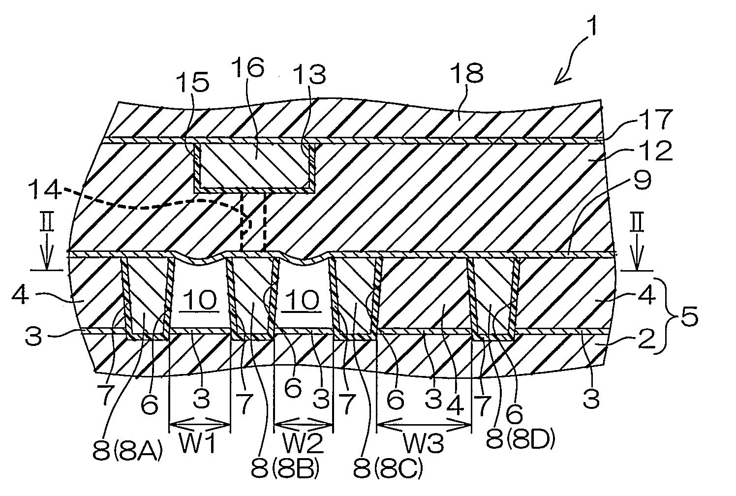
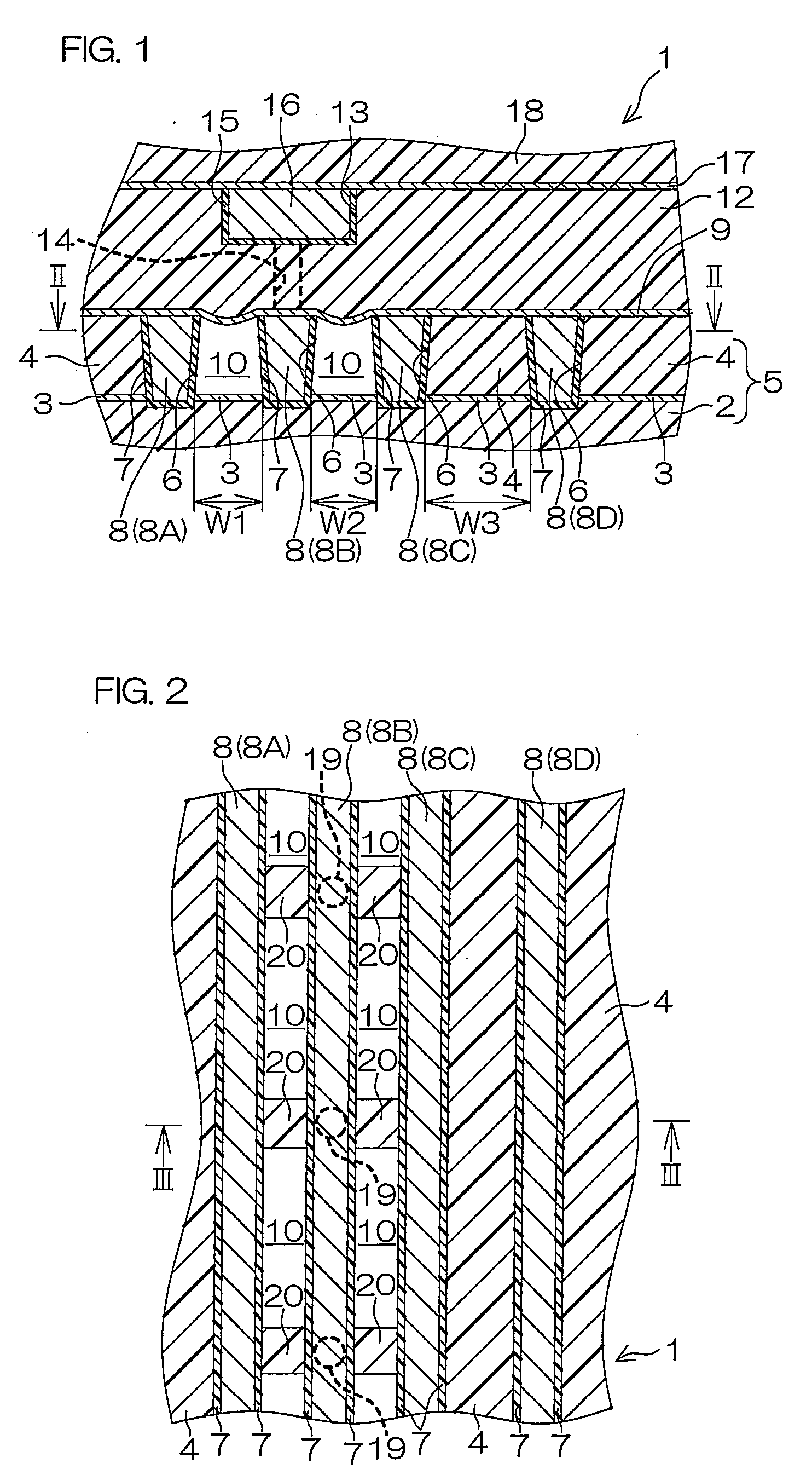
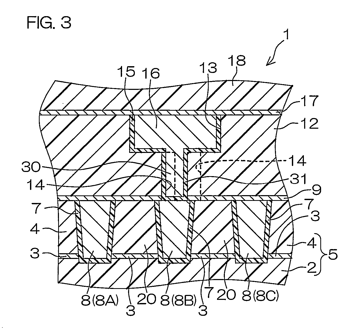
[0057]FIG. 1 is a sectional view schematically showing the structure of a semiconductor device 1 according to an embodiment of the present invention.

[0058]The semiconductor device 1 has a multilayer interconnection structure (consisting of two layers in this embodiment) of copper damascene wires 8 and 16 formed by the damascene process.

[0059]A lower insulating layer 2 made of SiO2 is stacked on a semiconductor substrate (not shown) forming a base of the semiconductor device 1. An etching stopper film 3 made of SiN (silicon nitride) is formed on a surface of the lower insulating layer 2. An upper insulating layer 4 made of SiO2 is stacked on the etching stopper film 3. The lower insulating layer 2 and the upper insulating layer 4 are vertically separated from each other by the etching stopper film 3, and constitute a first interlayer dielectric film 5.

[0060]Wiring trenches 6...


PUM


Abstract

The semiconductor device according to the present invention includes a first interlayer dielectric film, a plurality of copper damascene wires embedded in the first interlayer dielectric film at an interval from each other, and a diffusion preventing film stacked on the first interlayer dielectric film for preventing diffusion of copper contained in the copper damascene wires, while an air gap closed with the diffusion preventing film is formed between the copper damascene wires adjacent to each other by partially removing the first interlayer dielectric film from the space between these copper damascene wires.

Description

BACKGROUND OF THE INVENTION[0001]1. Field of the Invention[0002]The present invention relates to a semiconductor device having copper wires (copper damascene wires) formed by the damascene process and a method of manufacturing the same.[0003]2. Description of Related Art[0004]The damascene process is generally known as a technique for forming copper wires.[0005]FIG. 9 is a schematic sectional view showing the structure of a conventional semiconductor device having copper wires (copper damascene wires) formed by the damascene process.[0006]A first interlayer dielectric film 102 is stacked on a semiconductor substrate (not shown) forming a base of a semiconductor device 101. A plurality of trenches 103 are formed in the first interlayer dielectric film 102 at intervals in the horizontal direction in FIG. 9. The trenches 103 extend in a direction orthogonal to a plane of FIG. 9.[0007]Inner surfaces of the trenches 103 are covered with barrier films 104. Copper damascene wires 105 are e...

Claims


Application Information

Patent Timeline
IPC IPC(8): H01L23/532H01L21/4763
CPCH01L21/76816H01L21/7682H01L23/5222H01L2924/0002H01L2924/00
Inventor NAKAGAWA, RYOSUKE
Owner ROHM CO LTD
Why Eureka
Try Eureka