Semiconductor chip device having through-silicon-via (TSV) and its fabrication method

a technology of throughsilicon and semiconductor chips, applied in semiconductor devices, semiconductor/solid-state device details, electrical devices, etc., can solve the problems of low yield and high cost, easy filling, unstable process, etc., and achieve high-density connection, save fabrication costs, and simplify fabrication methods

Inactive Publication Date: 2009-05-21
POWERTECH TECHNOLOGY
View PDF3 Cites 69 Cited by
  • Summary
  • Abstract
  • Description
  • Claims
  • Application Information

AI Technical Summary

Benefits of technology

[0033]The though holes 340 are formed through the corresponding redistributed pads 321 and penetrate the chip 310 from the active surface 311 to the back surface 312. The insulation layer 350 is formed inside the through holes 340. Preferably, the insulation layer 350 is further formed over the back surface 312 of the chip 310 to protect the chip 310. Each flexible metal wire 360 has a first terminal 361 and a second terminal 362 where the first terminal 361 is bonded to the redistributed pad 321 and the second terminal 362 passes through the through hole 340 and protrudes from the back surface 312 of the chip 310. In the present embodiment, the first terminals 361 are ball bonds and the second terminals 362 are suspended to be movable with respect to the redistributed pad 321 so that the passivation layer on the back surface 312 of the chip 310 can b

Problems solved by technology

Due to the complicated fabrication method of TSV, the processes become unstable with lower yields and higher costs.
Since the conductive materials 160 are either plated copper or doped polycrystalline Silicon, it is not easy to fill the through holes 140 without any voids leading to poor resistance to stresses causing reliability issues.
Moreover, in order to fabricate the through holes 140 with the dielectric layer 113 and the conductive seed layer

Method used


Image

  • Semiconductor chip device having through-silicon-via (TSV) and its fabrication method
  • Semiconductor chip device having through-silicon-via (TSV) and its fabrication method
  • Semiconductor chip device having through-silicon-via (TSV) and its fabrication method

Examples


first embodiment

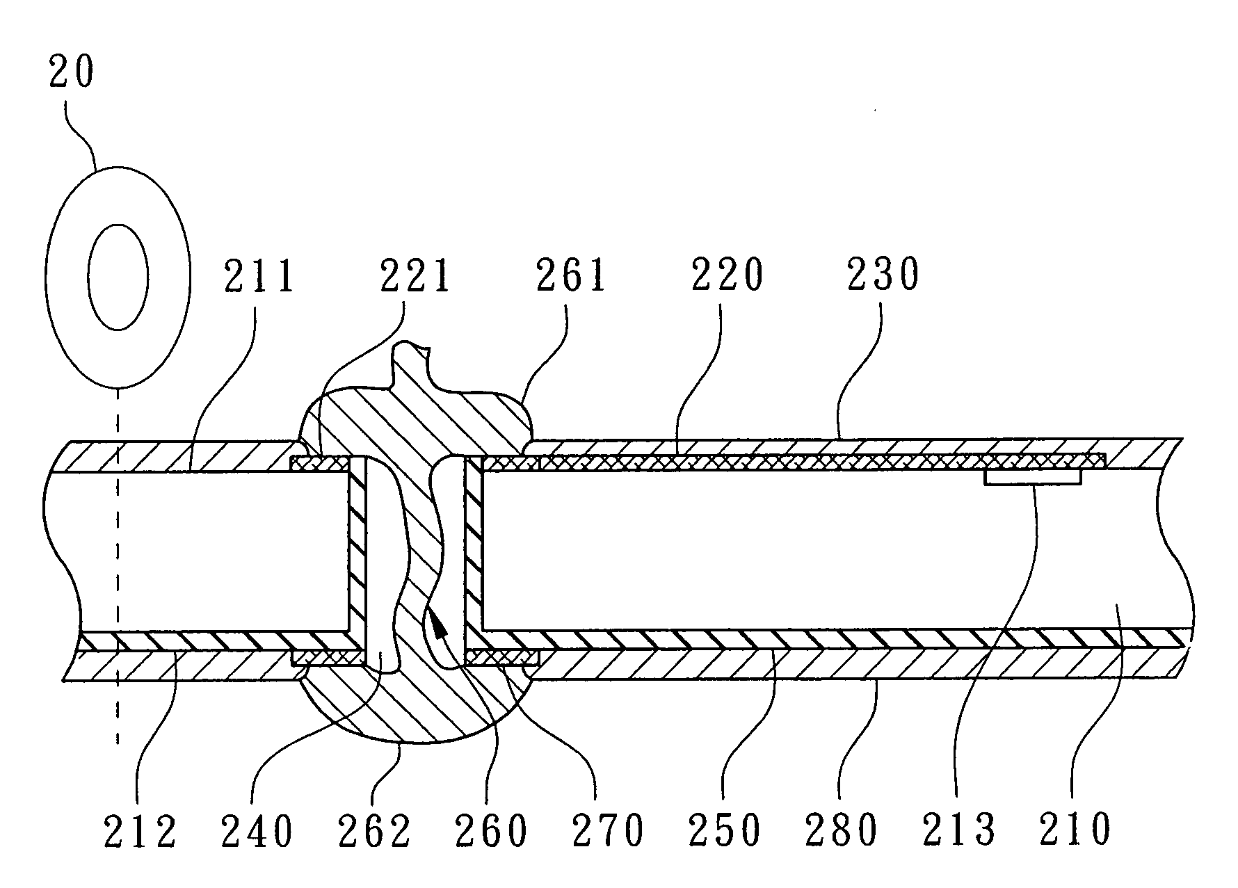
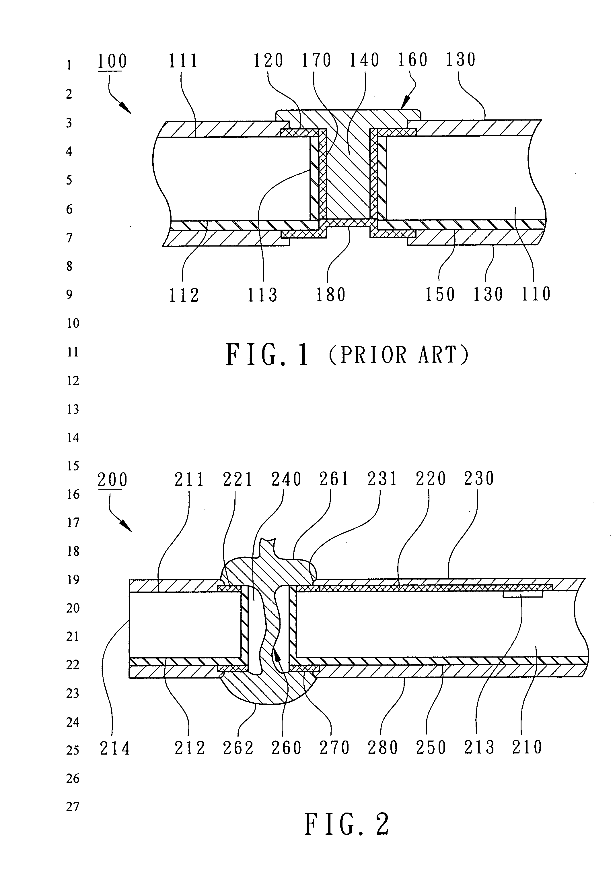
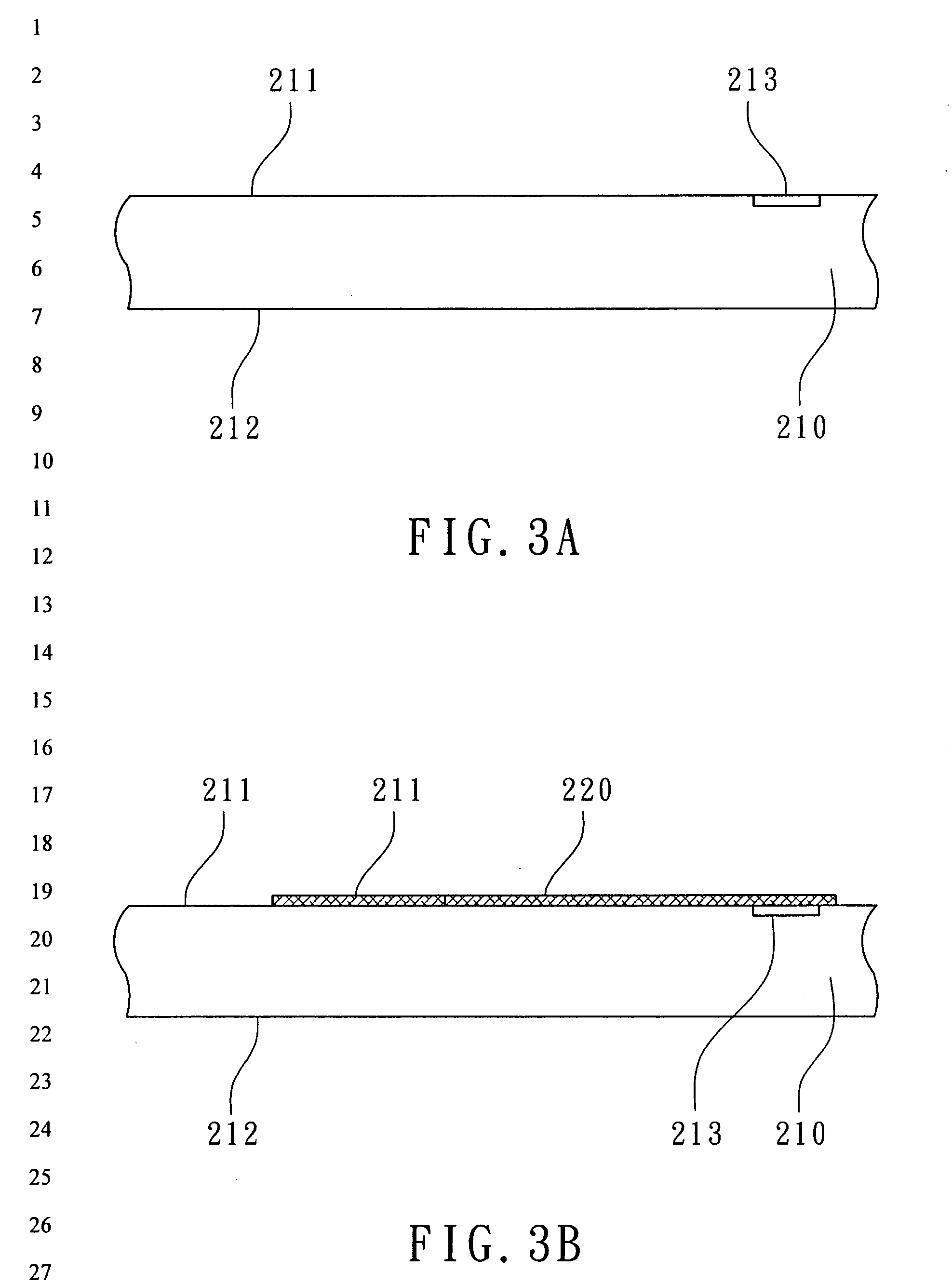
[0016]According to the present invention as shown in FIG. 2, a semiconductor device 200 with TSV primarily comprises a first chip 210, a redistributed trace layer 220, a first passivation layer 230, a plurality of through holes 240, an insulation layer 250, and a plurality of flexible metal wires 260. The chip 210 has an active surface 211, a back surface 212, and a plurality of bonding pads 213 formed on the active surface 211. Therein, only one of the through holes 240, one of the metal wires 260 and one of the bonding pads 213 are shown in FIG. 2. A variety of integrated circuits (IC) are formed on the active surface 211 and are electrically connected to the bonding pads 213. The material of the chip can be Si, GaAs, or other semiconductor materials.

[0017]The redistributed trace layer 220 is electrically conductive and is disposed on the active surface 211. The redistributed trace layer 220 includes a plurality of redistributed pads 221 electrically connected to the bonding pads ...

second embodiment

[0032]In the present invention, as shown in FIG. 6, another semiconductor device with TSV is revealed. The semiconductor device 300 primarily comprises a chip 310, a redistributed trace layer 320, a passivation layer 330, a plurality of through holes 340, an insulation layer 350, and a plurality of flexible metal wires 360. The chip 310 has an active surface 311, a back surface 312, and a plurality of bonding pads 313 formed on the active surface 311. The redistributed trace layer 320 is formed on the active surface 311 and includes a plurality of redistributed pads 321 electrically connected to the bonding pads 313. The passivation layer 330 is formed over the active surface 311 of the chip 310 to cover the redistributed trace layer 320. The passivation layer 330 further has a plurality of openings 331 to expose the corresponding redistributed pads 321 for bonding the flexible metal wires 360.

[0033]The though holes 340 are formed through the corresponding redistributed pads 321 and...


PUM


Abstract

A semiconductor device with TSV and its fabrication method are revealed. The semiconductor device primarily comprises a chip and a flexible metal wire inside. A redistributed trace layer and a passivation layer are formed on the active surface of the chip. A through hole penetrates the chip from the active surface to the back surface, in which an insulation layer is disposed. The flexible metal wire has a first terminal and a second terminal where the first terminal is bonded to a redistributed pad of the redistributed trace layer and the second terminal passes through the through hole and protrudes from the back surface of the chip. Therefore, the flexible metal wire passing through the chip has two protruded integral terminals to achieve high stress resistance TSV with lower costs for good electrical connections of vertical stacking chips.

Description

FIELD OF THE INVENTION[0001]The present invention relates to interconnection technologies within semiconductor chips, especially to semiconductor devices with Through-Silicon-Via (TSV) and its fabrication method.BACKGROUND OF THE INVENTION[0002]Integrated circuits (IC) are fabricated on the active surface of a chip. Conventionally the electrical terminals of a chip are only formed on the active surface such as bonding pads. In order to increase package densities within the smallest footprint, a plurality of chips are vertically stacked with electrical terminals disposed not only on the active surfaces of a chip but also on the back surface to increase the electrical interconnections between chips. This is why the Through-Silicon-Via (TSV) connection is developed, TSV's electrically connect vertically stacked chips through the electrical terminals on the active surfaces as well as on the back surfaces of the chips. However, the existing TSV technologies involve many front-end semicon...

Claims


Application Information

Patent Timeline
IPC IPC(8): H01L23/48H01L21/304
CPCH01L21/76898H01L23/481H01L2224/451H01L2224/136H01L2924/01033H01L2924/01006H01L2924/00013H01L2924/14H01L2924/10329H01L2924/014H01L2924/01082H01L2924/01078H01L2924/01029H01L24/11H01L24/12H01L24/16H01L24/48H01L24/78H01L24/85H01L25/0657H01L25/50H01L2224/1134H01L2224/13099H01L2224/131H01L2224/16H01L2224/4824H01L2224/78301H01L2224/85H01L2225/06513H01L2225/06541H01L2924/01014H01L2924/01027H01L2924/00014H01L2924/00H01L24/13H01L24/14H01L2224/11901H01L2224/13009H01L2224/14181H01L2224/16146H01L2224/05599H01L2224/45099
Inventor IWATA, RONALD TAKAO
Owner POWERTECH TECHNOLOGY
Why Eureka
Try Eureka