Stacking die package structure for semiconductor devices and method of the same

a technology of semiconductor devices and dies, applied in semiconductor devices, semiconductor/solid-state device details, electrical apparatus, etc., can solve the problems of not meeting the demand of producing smaller chips with high density elements on the chip, more bulky than desirable, and complicated semiconductors, etc., to achieve high reliability, low cost, and high performance.

Inactive Publication Date: 2009-05-21
ADVANCED CHIP ENG TECH
View PDF3 Cites 250 Cited by
  • Summary
  • Abstract
  • Description
  • Claims
  • Application Information

AI Technical Summary

Benefits of technology

[0008]An object of the present invention is to provide a semiconductor device package (chip assembly) with a chip and a conductive trace that provides a low cost, high performance and high reliability package.

Problems solved by technology

Such packages work well to protect IC dice, but they can be more bulky than desirable for certain multi-chip applications requiring compact die packaging.
As a semiconductor become more complicated, the traditional package technique, for example lead frame package, flex package, rigid package technique, can't meet the demand of producing smaller chip with high density elements on the chip.
Typical BGA packages include a convoluted signal path, giving rise to high impedance and an inefficient thermal path which results in poor thermal dissipation performance.
Recently, integrated circuit (chip) packaging technology is becoming a limiting factor for the development in packaged integrated circuits of higher performance.
It is because that the conventional designs include too many stacked dielectric layers and sealed compound, and the thermal dissipation is very poor, thereby decreasing the performance of the devices.
The mechanical property of the dielectric layers is not “elastic / softness”, it therefore leads to the CTE mismatching issue; It lacks of the stress releasing buffer layers contained therein.
Therefore, the scheme is not reliable during thermal cycle and the operation of the package.
Further, It is same die size scheme, the inter core does not include fiber glass and the inter-connecting through hole process is too complicated.

Method used


Image

  • Stacking die package structure for semiconductor devices and method of the same
  • Stacking die package structure for semiconductor devices and method of the same
  • Stacking die package structure for semiconductor devices and method of the same

Examples


second embodiment

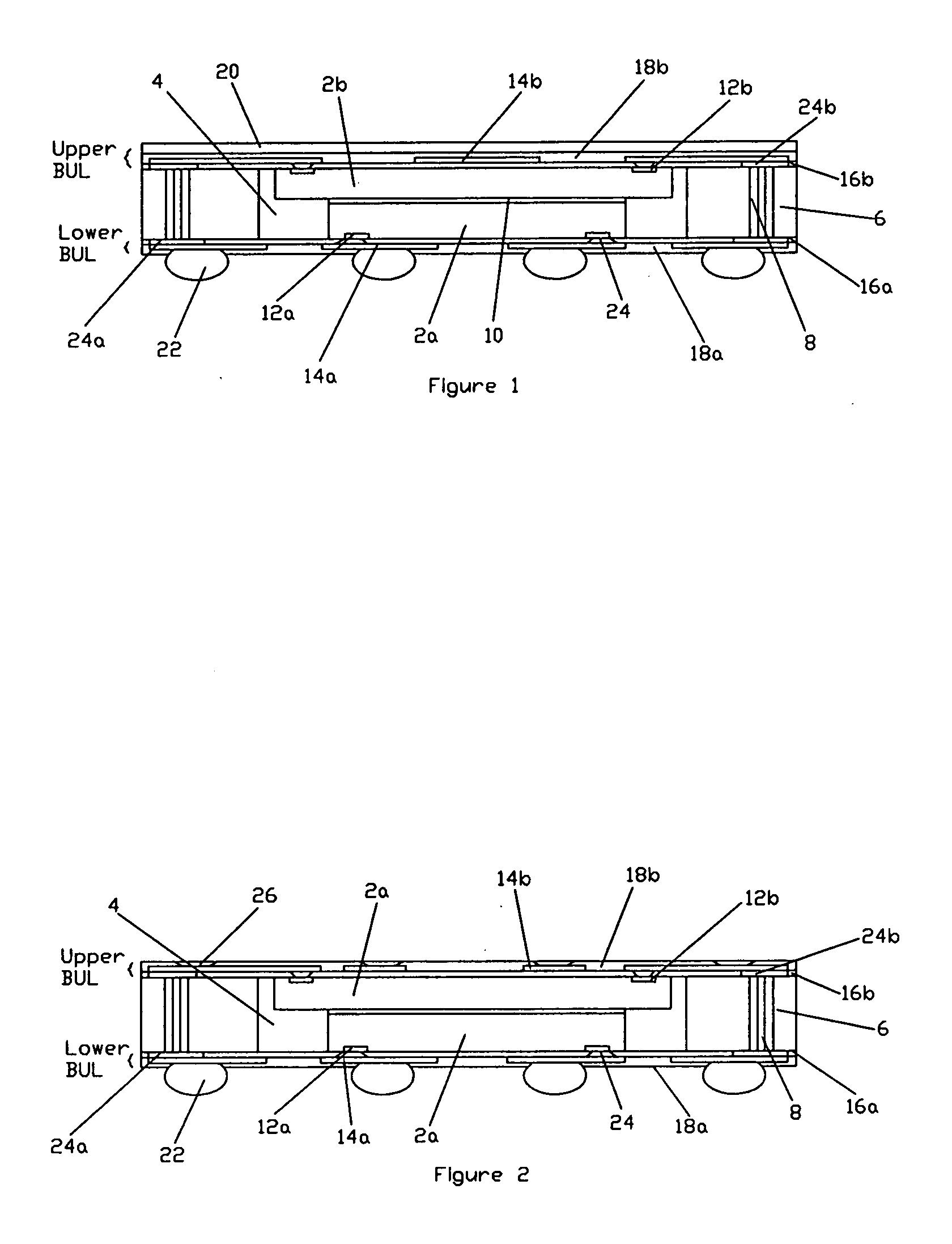
[0027]the present invention is similar to the last one embodiment as shown in FIG. 2. The embodiment omits the isolation base and includes top contact pads formed within the second dielectric layer 18b, it includes the UBM structure.

first embodiment

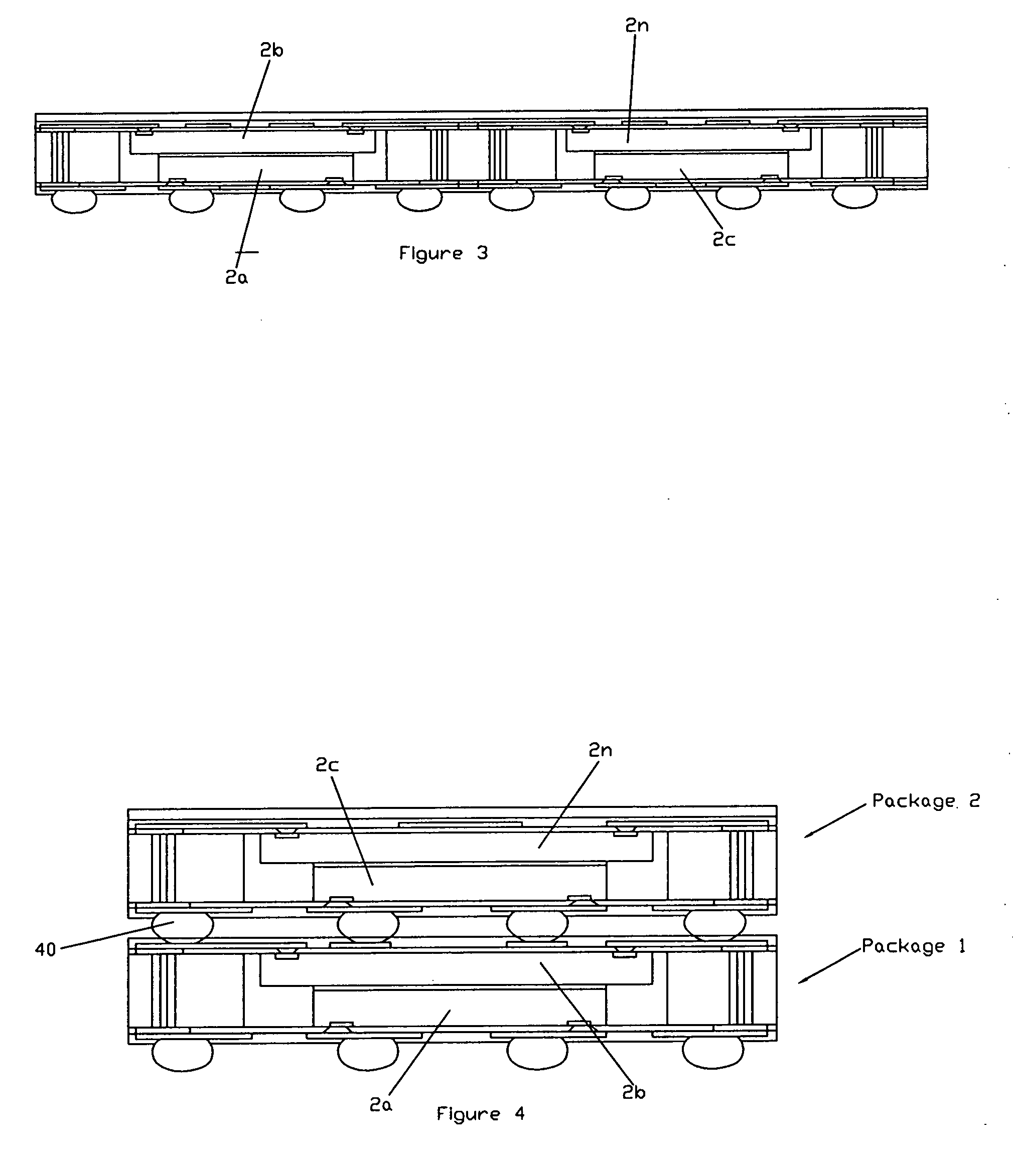
[0028]Alternatively, the embodiment includes two units of the first embodiment and configured by side-by-side scheme as shown in FIG. 3. It includes die 2a, 2b, 2c and 2n.

[0029]Alternatively, the die may be different type from others. It could be memory, ACIS, MCU, RF, Analog, and / or passive compounds etc.

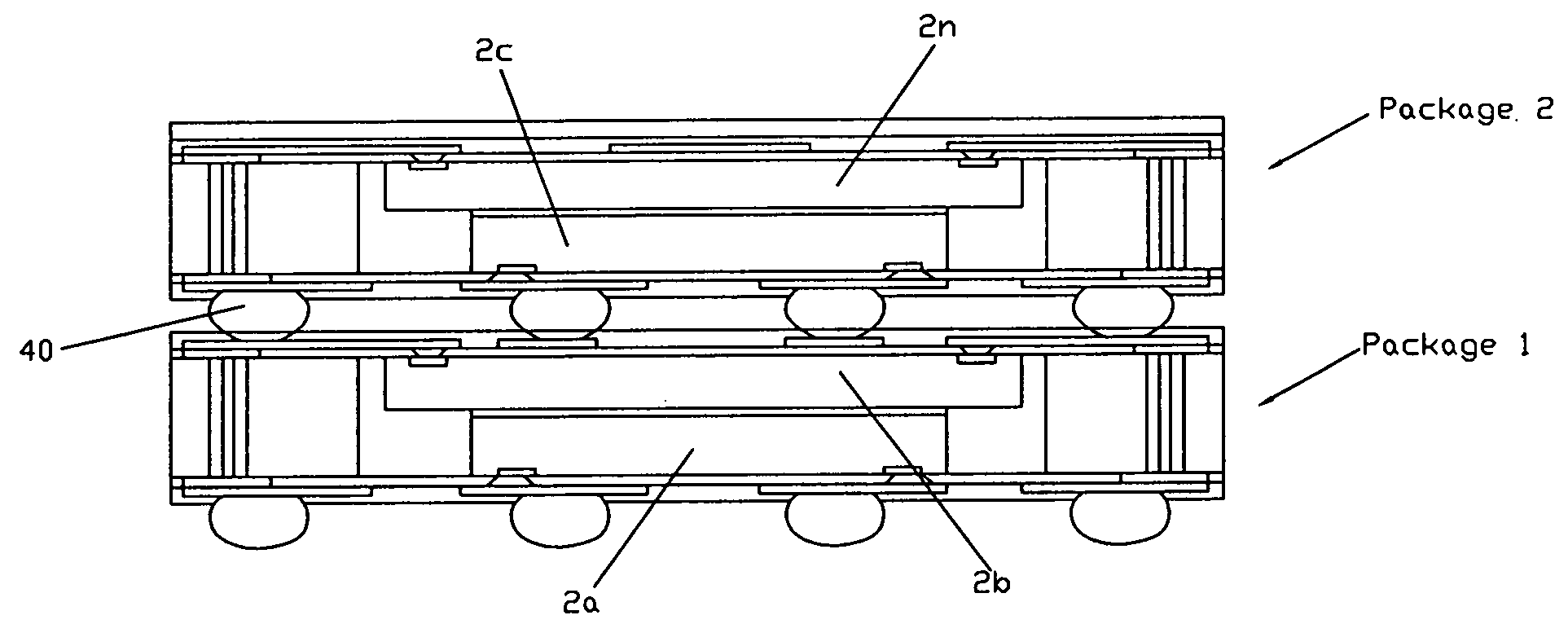
[0030]Please refer to FIG. 4, it is constructed by at least two units of the first embodiment, the solder (conductive) bumps 40 of the upper level package coupled to the upper RDL of the lower level package. Alternative, the isolation base is formed on the upper level unit.

[0031]The die size is decreased from top level to low level, subsequently. The smaller the chip is, the larger the core paste material is. Under the scheme, the core area of the lower die is the largest. It may strength the mechanical support to carry higher level package.

[0032]FIG. 5 illustrates the substrate 50 of the present invention. The substrate 50 includes pre-formed die receiving window (opening) 52 and...


PUM


Abstract

The present invention disclosed a first multi-die package structure for semiconductor devices, the structure comprises a substrate having die receiving window and inter-connecting through holes formed therein; a first level semiconductor die formed under a second level semiconductor die by back-to-back scheme and within the die receiving window, wherein the first multi-die package includes first level contact pads formed under the first level semiconductor die having a first level build up layer formed there-under to couple to a first bonding pads of the first level semiconductor die; a second level contact pads formed on the second level semiconductor die having a second level build up layer formed thereon to couple to second bonding pads of the second level semiconductor die; and conductive bumps formed under the first level build up layer.

Description

FIELD OF THE INVENTION[0001]This invention relates to a semiconductor package, and more particularly to a stacking die package for semiconductor devices.DESCRIPTION OF THE PRIOR ART[0002]Integrated circuit (IC) dice or “chips” are small, generally rectangular IC devices cut from a semiconductor wafer, such as a silicon wafer, on which multiple ICs have been fabricated. Traditionally, bare IC dice are packaged to protect them from corrosion by enclosing them in die packages. Such packages work well to protect IC dice, but they can be more bulky than desirable for certain multi-chip applications requiring compact die packaging. Improvements in IC packages are driven by industry demands for increased thermal and electrical performance and decreased size and cost of manufacture. In the field of semiconductor devices, the device density is increased and the device dimension is reduced, continuously. The demand for the packaging or interconnecting techniques in such high density devices i...

Claims


Application Information

Patent Timeline
Patent Type & Authority Applications(United States)
IPC IPC(8): H01L23/488H01L21/58
CPCH01L24/18H01L24/82H01L2924/07802H01L2924/10253H01L2224/73267H01L2224/32145H01L2225/1058H01L2225/1035H01L2924/01033H01L24/97H01L25/0652H01L25/0657H01L25/105H01L25/18H01L2224/18H01L2224/97H01L2225/06524H01L2225/06541H01L2924/01029H01L2924/01059H01L2924/01075H01L2924/01078H01L2924/01079H01L2924/01082H01L2924/14H01L2924/15311H01L2924/15331H01L2924/3011H01L2924/01005H01L2224/82H01L2924/00H01L2924/351H01L24/19H01L2224/04105H01L2224/12105
Inventor YANG, WEN-KUNWANG, CHI-YUHSU, HSIEN-WEN
Owner ADVANCED CHIP ENG TECH
Why Eureka
Try Eureka