Organic light-emitting device

a light-emitting device and organic technology, applied in the direction of discharge tube luminescnet screen, discharge tube/lamp details, electric discharge lamps, etc., can solve the problems of large difference in affinity level between the n the p-type organic compound layer, and achieve satisfactory emission. , the effect of reducing power consumption, long life and high efficiency

Inactive Publication Date: 2009-05-21
IDEMITSU KOSAN CO LTD
View PDF10 Cites 19 Cited by
  • Summary
  • Abstract
  • Description
  • Claims
  • Application Information

AI Technical Summary

Benefits of technology

[0014]According to the invention, an organic light-emitting device which has a hig

Problems solved by technology

However, in this device configuration, difference in affinity level between the n-type organic compound layer and the p-type organic compound layer is large.
In this device configuration, however, there is a large difference in electron

Method used


Image

  • Organic light-emitting device
  • Organic light-emitting device
  • Organic light-emitting device

Examples


example 1

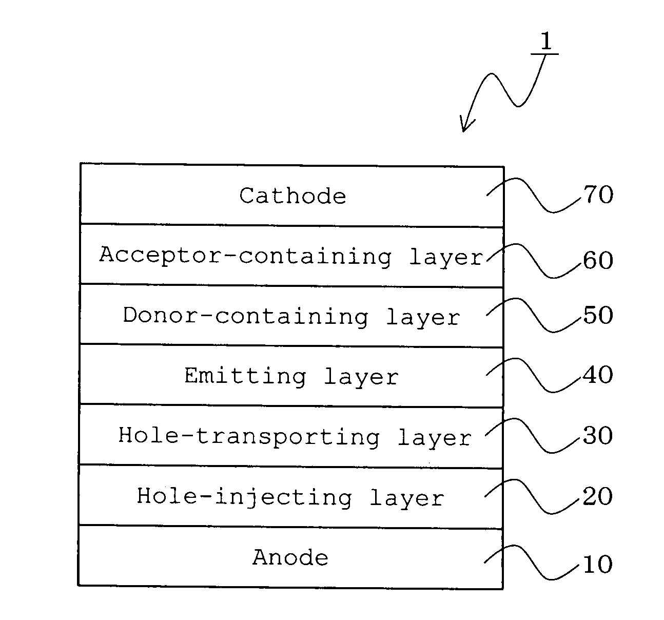
[0095]An ITO film was formed on a 0.7 mm-thick glass substrate by sputtering in a thickness of 130 nm. The substrate was subjected to ultrasonic cleaning in isopropyl alcohol for 5 minutes, and cleaned with ultraviolet ozone for 30 minutes. Then, the substrate with the ITO electrode was mounted on a substrate holder in a vacuum vapor deposition apparatus.

[0096]TPD232 as a material for a hole-injecting layer, TBDB as a material for a hole-transporting layer, BH as a host material for an emitting layer, BD as a blue emitting material, Alq as an electron-transporting material, Li as a donor, (CN)2TCNQ as an acceptor and Al as a cathode material were mounted on respective molybdenum heating boats in advance.

[0097]First, a TPD232 film which functioned as the hole-injecting layer was formed in a thickness of 60 nm. After forming the hole-injecting layer, a TBDB film which functioned as the hole-transporting layer was formed in a thickness of 20 nm. Then, the compound BH and the compound B...

example 2

[0099]An organic light-emitting device was fabricated in the same manner as in Example 1, except that, in Example 1, the donor-containing layer (light transmittance: 90%, specific resistance: 1014 Ω·cm) was formed by using Liq as the donor instead of Li.

[0100]Evaluation was conducted for the resulting organic light-emitting device. The results are shown in Table 1.

example 3

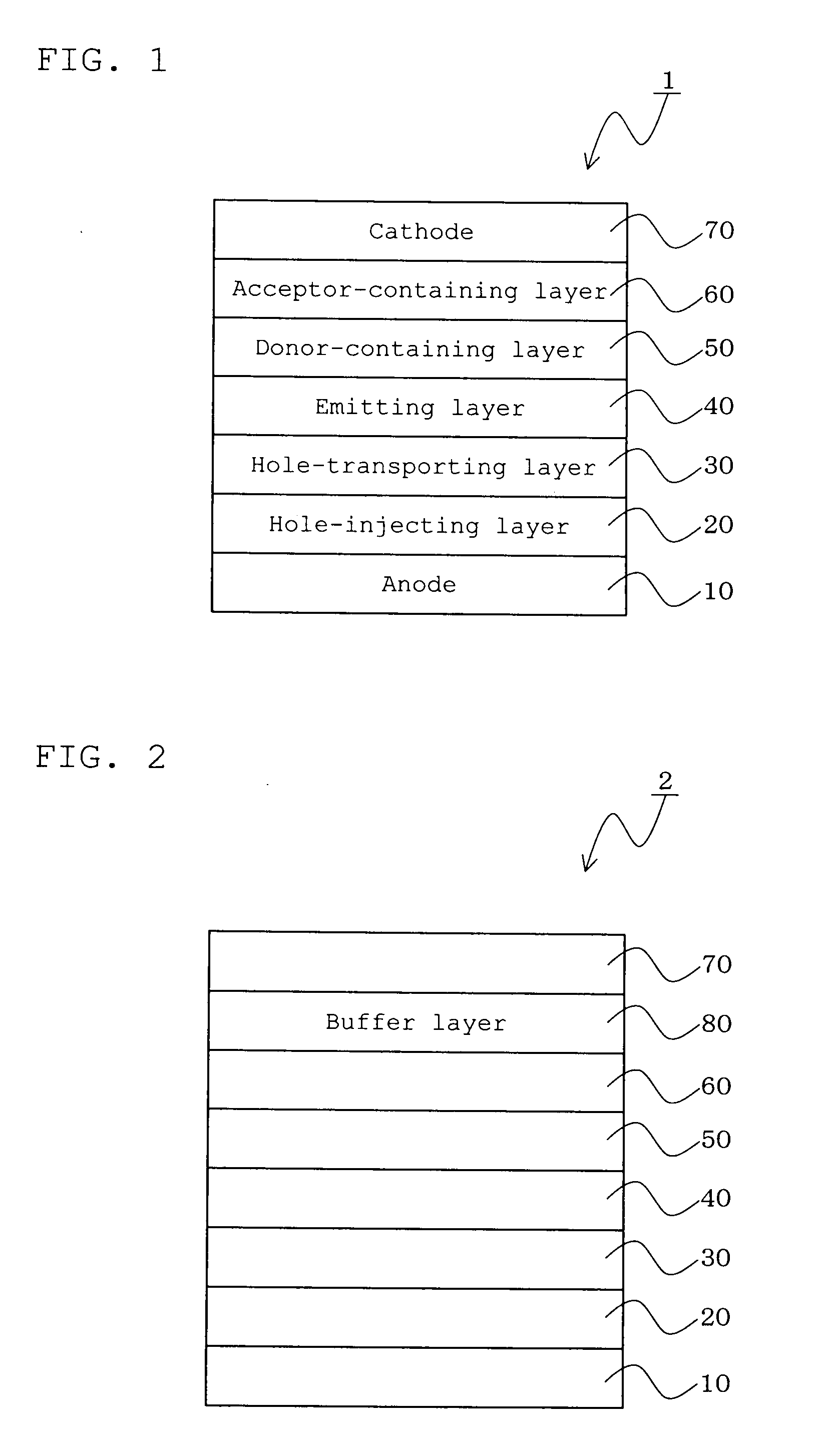
[0101]An organic light-emitting device was fabricated in the same manner as in Example 2, except that, in Example 1, after formation of the acceptor layer, a 10 nm-thick buffer layer was formed using MoOx (x=2 to 3) as a material for a buffer layer, followed by the formation of an Al film (cathode).

[0102]Evaluation was conducted for the resulting organic light-emitting device. The results are shown in Table 1.


PUM


Abstract

An organic light-emitting device (1) including, arranged in the following order: an anode (10), an emitting layer (40), a donor-containing layer (50), an acceptor-containing layer (60) and a cathode (70), the donor-containing layer (50) containing at least one selected from a donor metal, a donor metal compound and a donor metal complex.

Description

TECHNICAL FIELD[0001]The invention relates to an organic light-emitting device, in particular, to an organic electroluminescence (EL) device.BACKGROUND ART[0002]An EL device utilizing electroluminescence has a high degree of visibility due to the self-emitting nature thereof. In addition, being a perfect solid device, it has benefits such as excellent impact resistance. For these reasons, use of an EL device as a light-emitting device in various displays has attracted attention.[0003]The EL device is divided into an inorganic EL device using an inorganic compound as an emitting material, and an organic EL device using an organic compound as an emitting material. Of these, an organic EL device has been developed as a next-generation emitting device, since it can significantly reduce an applied voltage, can easily attain full-color display, consumes only a small amount of power and is capable of performing plane emission.[0004]Although an organic EL device basically comprises an anode...

Claims


Application Information

Patent Timeline
IPC IPC(8): H01L51/52
CPCH05B33/14H01L51/5052H10K50/155H10K50/165H05B33/20H10K50/00
Inventor FUKUOKA, KENICHIHOSOKAWA, CHISHIOMORISHITA, HIRONOBUKUMA, HITOSHI
Owner IDEMITSU KOSAN CO LTD
Why Eureka
Try Eureka