Semiconductor power device package having a lead frame-based integrated inductor

a technology of integrated inductor and power device, which is applied in the direction of transformer/inductance details, basic electric elements, inductance, etc., can solve the problems of high component cost, inconvenient use, and inability to meet the requirements of a single power converter, etc., to achieve low cost and space efficiency, high inductance, and low dc resistance

Active Publication Date: 2009-05-28
ALPHA & OMEGA SEMICON INC
View PDF5 Cites 29 Cited by
  • Summary
  • Abstract
  • Description
  • Claims
  • Application Information

AI Technical Summary

Benefits of technology

[0010]The semiconductor power device package having an integrated inductor of the invention fulfills these needs and provides advantages over the prior art by utilizing the lead frame and metal connections such as bonding wires, in combination with an inductor core, to provide an integrated inductor having high inductance and low DC resistance and which is low-cost and space efficient. Alternatively, two lead frames, in combination with an inductor core, are utilized to provide the integrated inductor. The entire structure is protected by a molding compound to protect the integrated inductor and IC chip.

Problems solved by technology

Power converters implemented in this way suffer the disadvantages of having higher component cost and of requiring more printed circuit board space.
The large package size demonstrates the challenge of finding a discrete inductor small enough to be co-packaged with the power IC, yet having a large inductance, small DC resistance and large rated current capable of meeting power conversion requirements.
Furthermore, utilizing a discrete inductor is not cost effective as the cost of the final package includes duplicative component assembly costs (the cost of assembling the discrete inductor and of the final package) and the additional cost of incorporating the discrete inductor in the final package.
Disadvantageously, the induction element is exposed allowing the fragile substrate material to be easily damaged.
To achieve high inductance, a large die is required resulting in a high cost and a large package.
Furthermore, complex processing is necessary in order to fabricate the planar magnetic layers.
These designs are suitable for RF applications, but lacking magnetic core material, they provide relatively small inductances that are not sufficient for power conversion applications.

Method used


Image

  • Semiconductor power device package having a lead frame-based integrated inductor
  • Semiconductor power device package having a lead frame-based integrated inductor
  • Semiconductor power device package having a lead frame-based integrated inductor

Examples


first embodiment

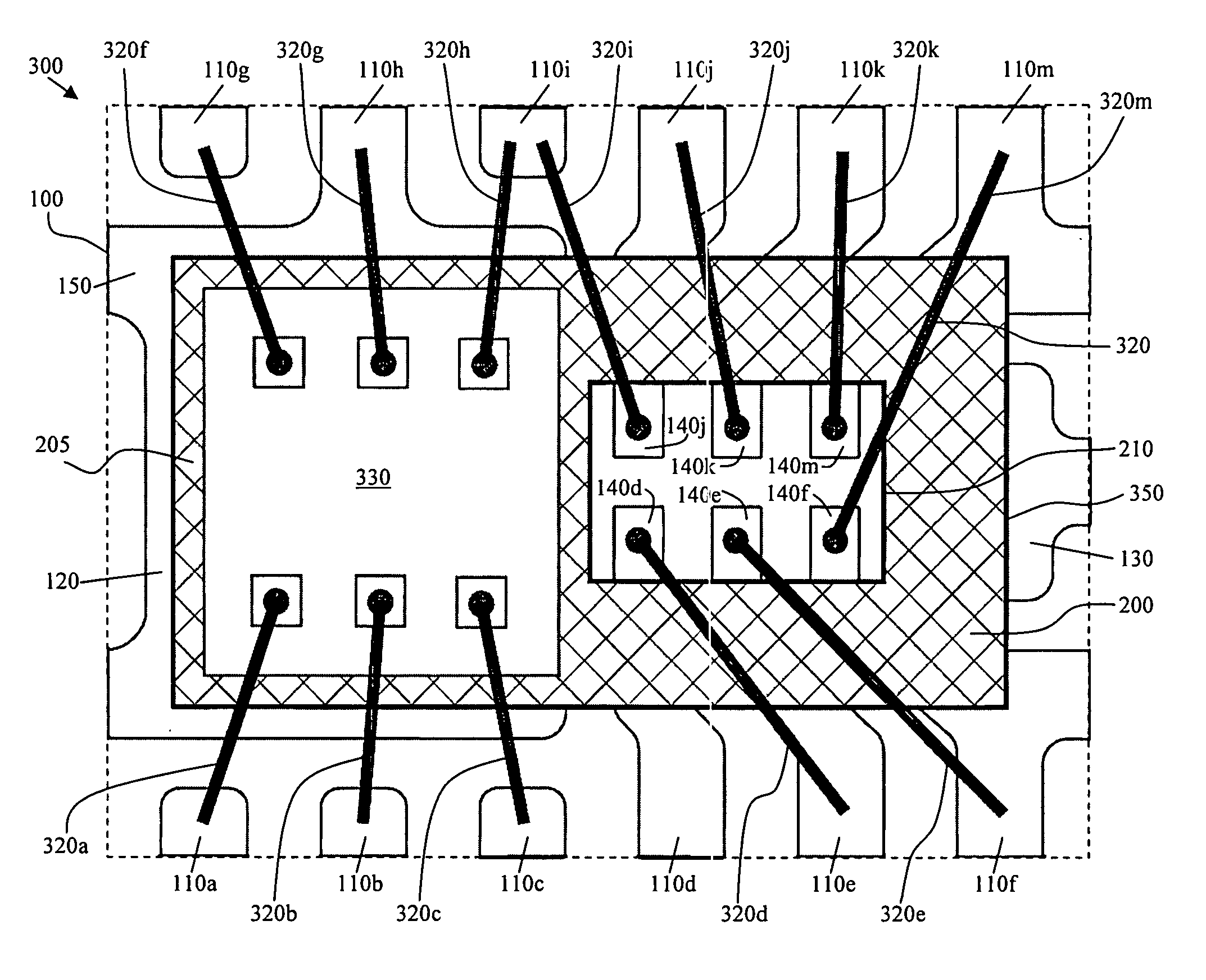
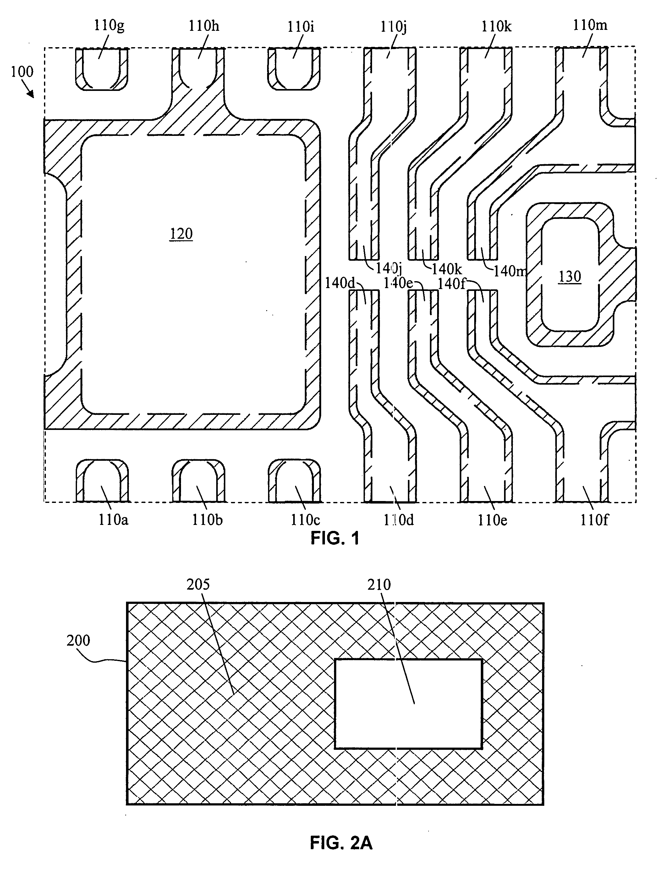
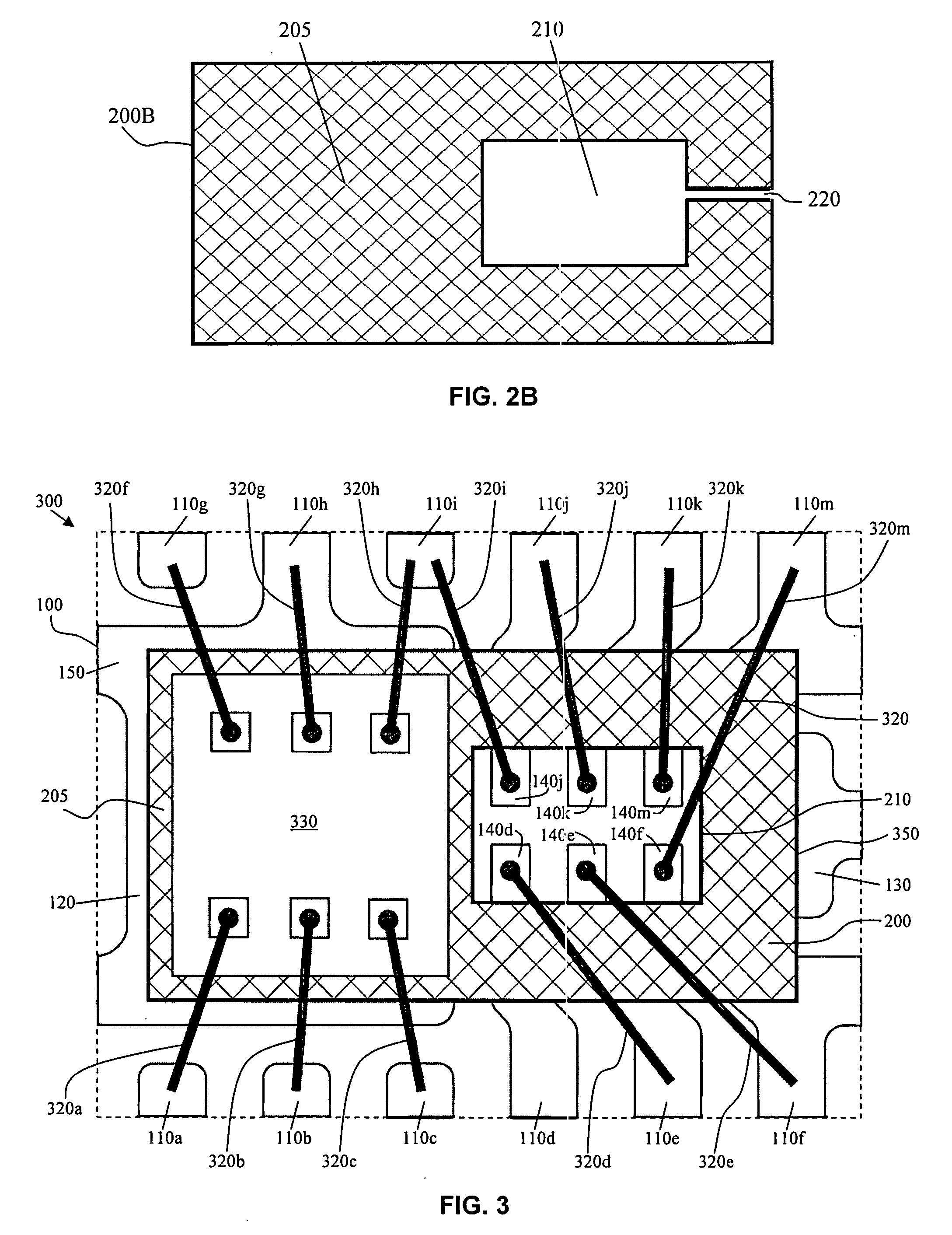
[0058]the invention is shown in FIG. 3 and includes a semiconductor power device package 300 having a lead frame-based integrated inductor 350. The inductor 350 is comprised of the inductor core 200, a plurality of leads of the lead frame 100 and metal connections such as bonding wires 320d, 320e, 320i, 320j, 320k and 320m coupled between the plurality of leads as shown. The inductor core 200 is attached to a top surface 150 of the lead frame 100 and is supported by the large pad 120 and the small pad 130. The inductor core 200 is disposed on the top surface 150 of the lead frame 100 in such manner that lead ends 140d-140f and 140j-140m are accessible through the offset window 210.

[0059]Bonding wires 320 couple a plurality of adjacent leads of the lead frame 100 to provide a closed magnetic circuit around the inductor core 200. Bonding wire 320d couples the end 140d of the lead 110d to the adjacent lead 110e, the bonding wire 320d, the lead 110d and the adjacent lead 110e forming a ...

second embodiment

[0063]the invention is shown in FIG. 4 and includes a semiconductor power device package 400 having a lead frame-based integrated inductor 450. The inductor 450 is comprised of the inductor core 200, a plurality of leads of the lead frame 100, and metal connections such as bonding wires 320d, 320e, 320i, 320j, 320k and 320m. A connection chip 500 provides electrical connection between bonding wires 320d, 320e, 320i, 320j, 320k and 320m and lead ends by means of vias 510a-510f formed in the connection chip 500 (FIG. 5 and FIG. 6). The inductor core 200 is attached to the top surface 150 of the lead frame 100 and is supported by the large pad 120 and the small pad 130. The inductor core 200 is disposed on the top surface 150 of the lead frame 100 in such manner that lead ends 140d-140f and 140j-140m are accessible through the offset window 210.

[0064]Connection chip 500 is sized and configured to fit within the offset window 210. Connection chip 500 is used to facilitate wire bonding i...

third embodiment

[0069]the invention is shown in FIG. 16 and includes a semiconductor power device package 1600 having a lead frame-based integrated inductor 1650 (FIG. 16). Semiconductor power device package 1600 is comprised of a bottom portion 900 (FIG. 9) and a top lead frame 1400 (FIG. 14 and FIG. 15). The bottom portion 900 comprises of a bottom lead frame 100, the inductor core 200, a bumped power IC 1000, and a connection chip 1200. The inductor 1650 is comprised of the inductor core 200, a plurality of adjacent leads of the lead frame 100 and a plurality of adjacent leads of the top lead frame 1400. A double-sided bumped connection chip 1200 (FIG. 12 and FIG. 13) provides electrical connection by means of vias formed in the connection chip 1200 (vias 1210a-1210c are shown in FIG. 13). The inductor core 200 is attached to the top surface 150 of the lead frame 100 and is supported by the large pad 120 and the small pad 130. The inductor core 200 is disposed on the top surface 150 of the lead ...


PUM


Abstract

A semiconductor power device package having a lead frame-based integrated inductor is disclosed. The semiconductor power device package includes a lead frame having a plurality of leads, a inductor core attached to the lead frame such that a plurality of lead ends are exposed through a window formed in the inductor core, a plurality of bonding wires, ones of the plurality of bonding wires coupling each of the plurality of lead ends to adjacent leads about the inductor core to form the inductor, and a power integrated circuit coupled to the inductor. In alternative embodiments, a top lead frame couples each of the plurality of lead ends to adjacent leads about the inductor core by means of a connection chip.

Description

BACKGROUND OF THE INVENTION[0001]1. Field of the Invention[0002]The present invention generally relates to semiconductor power devices and more particularly to a semiconductor power device package having a lead frame-based integrated inductor.[0003]2. Description of Related Art[0004]It is well known to include a discrete inductor on the printed circuit board when implementing a power converter circuit. For example, the Analogic™ TECH 1 MHz 400 mA Step-Down Converter (AAT1143) requires the use of a discrete inductor. Power converters implemented in this way suffer the disadvantages of having higher component cost and of requiring more printed circuit board space.[0005]Discrete inductors co-packaged with power ICs and other components are also well known. For example, the LTM®4600 DC / DC power converter available from Linear Technology Corporation of Milpitas, Calif., includes a built-in inductor in a 15 mm×15 mm×2.8 mm package. The large package size demonstrates the challenge of find...

Claims


Application Information

Patent Timeline
Patent Type & Authority Applications(United States)
IPC IPC(8): H01L23/495H01L21/60
CPCH01F17/0033H01F2027/2814H01L2924/1461H01L2924/014H01L2924/01033H01L2924/01019H01L2924/01006H01L24/48H01L2924/30107H01L2924/19107H01L2924/14H01L2924/01082H01L2924/0105H01L2924/01029H01L2224/49171H01L2224/48465H01L2224/48247H01L23/495H01L24/49H01L2224/48091H01L2924/00014H01L2924/00H01L2924/181H01L2224/05553H01L2224/05554H01L2924/10161H01F27/2866H01F27/40H01L2224/45099H01L2224/05599
Inventor FENG, TAOZHANG, XIAOTIANHEBERT, FRANCOIS
Owner ALPHA & OMEGA SEMICON INC
Why Eureka
Try Eureka