Method of manufacturing semiconductor element

a manufacturing method and semiconductor technology, applied in semiconductor lasers, laser details, electrical equipment, etc., can solve the problems of inability to apply a high-precision dividing method, inability to achieve stable products, and inability to achieve high-precision dividing methods, etc., to achieve high accuracy and improve product yield.

Active Publication Date: 2009-05-28
NICHIA CORP
View PDF4 Cites 41 Cited by
  • Summary
  • Abstract
  • Description
  • Claims
  • Application Information

AI Technical Summary

Benefits of technology

[0028]According to a method of manufacturing a semiconductor element of the present invention, two kinds of cleavage auxiliary grooves are adjacently provided along a proposed cleavage locati

Problems solved by technology

However, even if cleavage is performed by using such grooves (as in JP 2004-327879A), cleaved planes may deviate from the intended locations due to dislocation density and crystal defects and the like within the substrate or nitride semiconductor layers, making it difficult to achieve a stable product yield
On the other hand, this method cannot be applied to a high-precision dividing.
In the cases where the predetermined cleavage lines are formed by typical scribing or by laser processing, cleavage locations may be contaminated, damaged, or deformed by s

Method used


Image

  • Method of manufacturing semiconductor element
  • Method of manufacturing semiconductor element
  • Method of manufacturing semiconductor element

Examples


example 1

[0116]Example 1 of the present invention illustrates a structure of a laser element and a method of manufacturing the same.

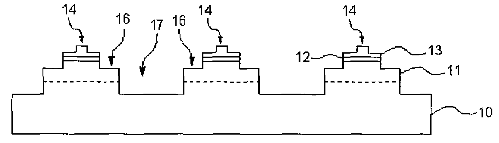
[0117]First, a nitride substrate made of n-type GaN with a thickness of 400 μm is set in a MOVPE reaction vessel, and a nitride semiconductor layer to be described below is stacked to form an element structure. The surface of the substrate is C-plane and the semiconductor crystal to be described below is grown along the c-axis.

[0118]As a first conductive type semiconductor layer 11, a first layer of n-Al0.02Ga0.98N doped with about 1018 / cm3 of Si and a second layer of n-In0.04Ga0.96N doped with about 1018 / cm3 of Si are grown, and thereon, an n-type cladding layer of Al0.11Ga0.89N doped with about 1018 / cm3 of Si, and an n-side optical guide layer of undoped Al0.06Ga0.94N are grown. Next, as an active layer 12, a barrier layer of Al0.15Ga0.85N doped with about 1019 / cm3 of Si, an undoped well layer of In0.01Ga0.99N, and a barrier layer of Al0.15Ga0.85N are grown to...

example 2

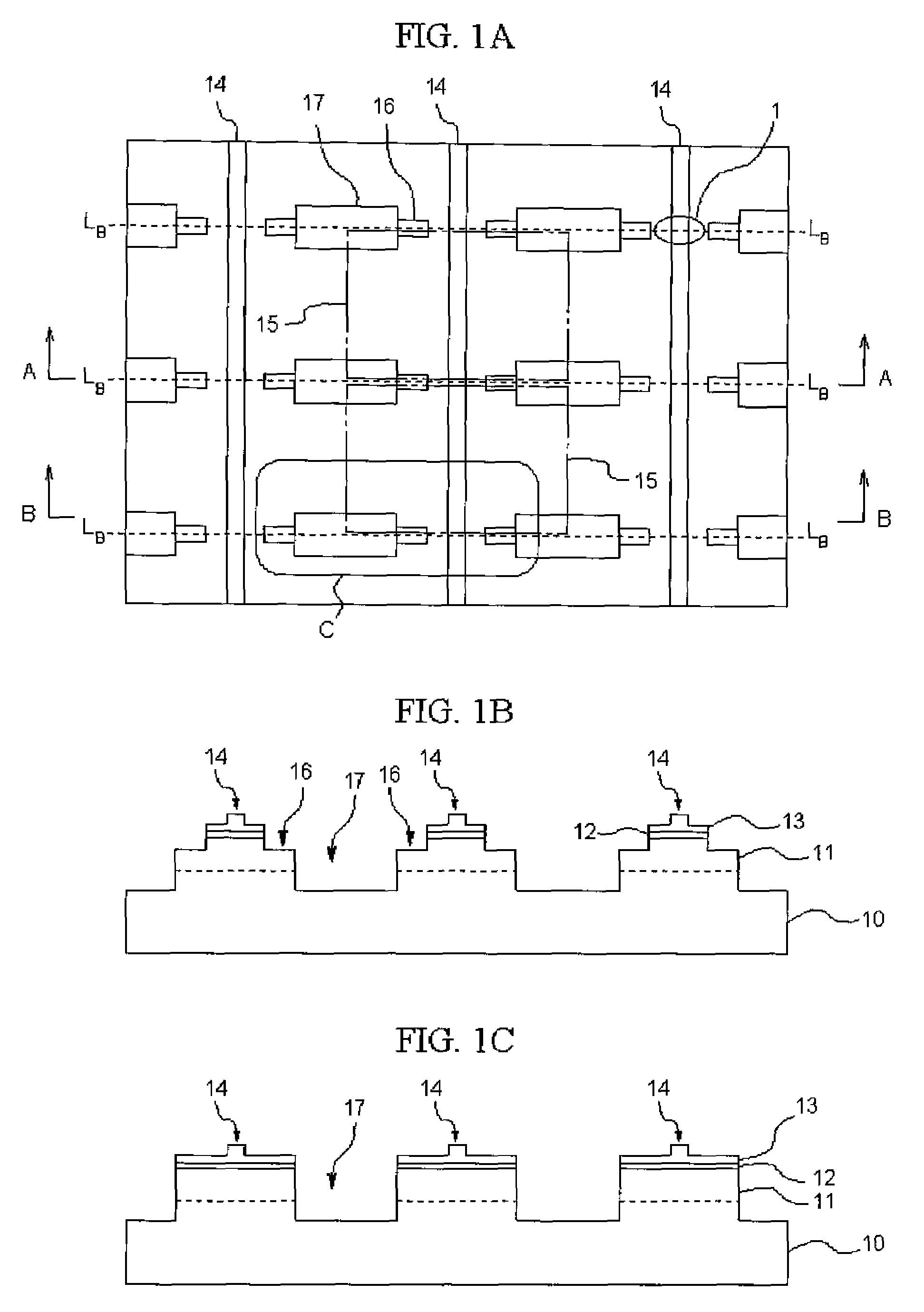
[0131]In a similar manner as in Example 1, a wafer having a element structure of a nitride semiconductor layer on a substrate is taken out of a reaction vessel, a mask pattern of a desired shape is disposed on a p-side contact layer, and using the mask pattern, an etching is performed from the p-side contact layer side to a part of an n-side cladding layer to form an auxiliary groove 30. Different from that in Example 1, by forming an exposed region of the n-side cladding layer, as shown in FIG. 3, island-shaped portions 28 and three first auxiliary grooves 30A to 30C which are interposed between the island portions 28 and divided by the exposed region 29B. Here, the exposed region 29B is formed so as to surround the second auxiliary groove 31, and divides the element regions from each other, and divides the second auxiliary groove and the element region 15 from each other. Herein, the width (length in the cleavage direction) of the exposed region 29A is about 30 μm, and in the expo...

example 3

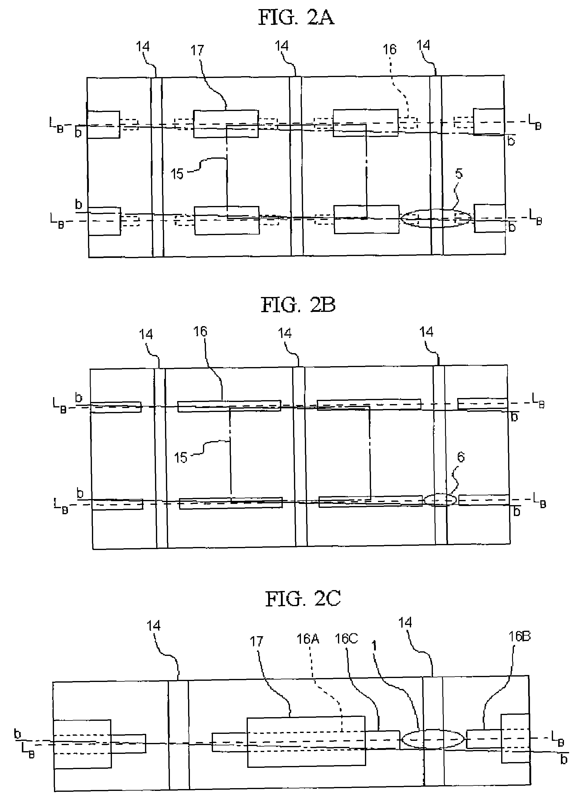
[0139]The element is formed in a similar manner as in Example 1, except that a semiconductor substrate having dislocation-concentrated regions in a stripe-shaped distribution so as to interpose two ridges, and the second auxiliary grooves are provided dividing the region with a wider length (length in dividing direction) with respect to the region.

[0140]As described above, in a case of dividing of a substrate with a region having largely different crystallinity by crossing a plurality of times, an adverse effect caused by dividing across the region can be suppressed by forming a second auxiliary groove cross-linking the element regions at the both sides of the region.


PUM


Abstract

A step of forming a first auxiliary groove in a semiconductor element structure provided on a semiconductor substrate, a step of forming a second auxiliary groove in the semiconductor element structure, and a step of dividing the semiconductor substrate and the semiconductor element structure in a direction along the first auxiliary groove and the second auxiliary groove are provided, and in the dividing direction, a plurality of the second auxiliary grooves are arranged spaced apart from each other, and at least two first auxiliary grooves are arranged spaced apart from each other between at least a pair of adjacent second auxiliary grooves, and in the dividing step, a separation region interposed between the two first auxiliary grooves is divided, so as to improve such accuracy and suppress the problems such as a damage of the end surface due to cleavage of the substrate.

Description

BACKGROUND OF THE INVENTION[0001]1. Field of the Invention[0002]The present invention relates to a method of manufacturing a semiconductor element, and particularly to a method of manufacturing a nitride semiconductor laser element.[0003]2. Discussion of the Related Art[0004]A nitride semiconductor is formed by a compound semiconductor of InxAlyGa1-x-yN (0≦x, 0≦y, and 0≦x+y≦1), various demands for the semiconductor laser elements using such a nitride semiconductor have been increasing, for use in optical disc systems capable of recording and reproducing large-volume, high-density information such as a next-generation DVD, and for use in electric appliances such as personal computers. For this, many studies have been conducted to manufacture the semiconductor laser elements using such a nitride semiconductor with a good reproducibility while maintaining their stable properties.[0005]For example, in order to prevent chipping and cracking of the ridge due to propagation from a dislocat...

Claims


Application Information

Patent Timeline
IPC IPC(8): H01L21/50
CPCH01S5/0202H01S5/028H01S2304/12H01S5/32341H01S2301/176H01S5/22H01S5/323
Inventor SAKAMOTO, KEIJISAKATA, HIROKI
Owner NICHIA CORP
Why Eureka
Try Eureka