
Methods and apparatus for packaging electronic components

a technology for electronic components and packaging, applied in the manufacture of electric discharge tubes/lamps, electrode systems, discharge tubes luminescnet screens, etc., can solve the problems of increased difficulty in sealing of larger-sized oled devices, such as full-size tvs having a diagonal of 14 inches or larger, and are susceptible to damag

Inactive Publication Date: 2009-06-04
CORNING INC
View PDF17 Cites 53 Cited by
  • Summary
  • Abstract
  • Description
  • Claims
  • Application Information

AI Technical Summary

Benefits of technology

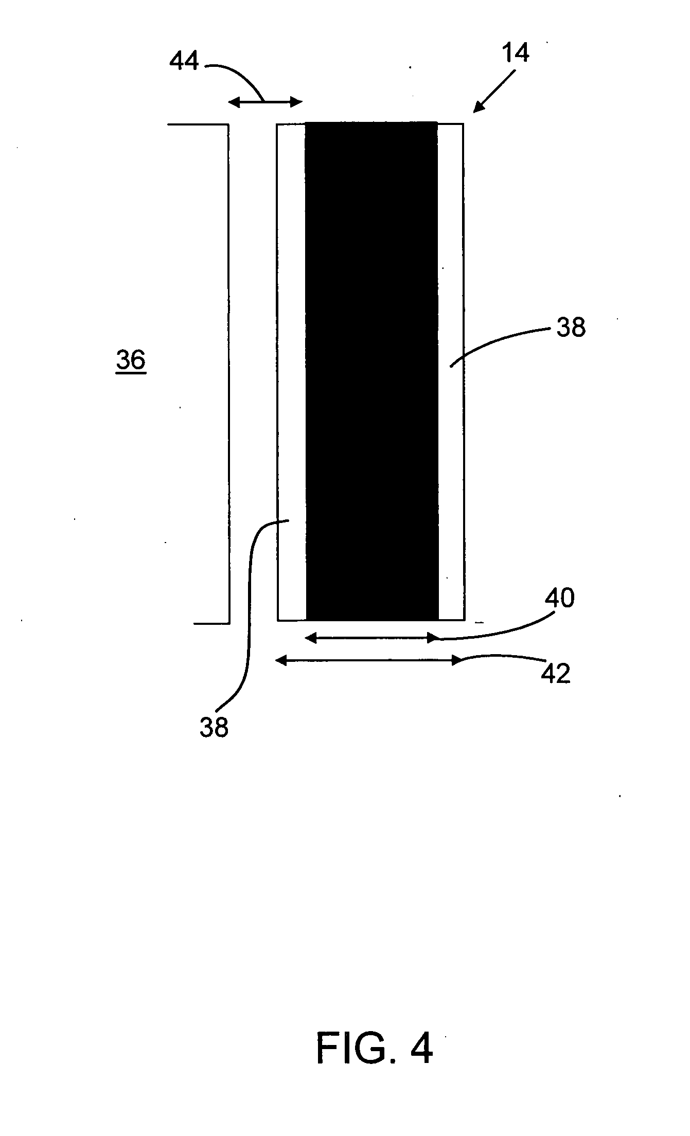
[0020]In certain embodiments of the first and second aspects of the invention, Wseal-min is less than or equal to 7 millimeters. Preferably, Wseal-min is less than or equal to 6 millimeters and greater than or equal to 3 millimeters, e.g., Wseal-min approximately equals 5 millimeters.
[0021]In accordance with a third aspect, the invention provides a package comprising a first glass substrate (12), a second glass substrate (16), a wall (14) that comprises a sintered glass frit and separates th

Problems solved by technology

However, OLEDs are susceptible to damage resulting from exposure to oxygen and moisture.
Such exposure may lead to a reduction in the useful life of the light emitting device.
The sealing of larger size OLED devices, such as full-size TVs having a diagonal of, for example, 14 inches or larger, is more challenging than sealing smaller OLED devices, such as those used in cell phones, PDAs and other mobile electronic devices.
In comparison to small devices, larger size OLED devices such as TVs require longer service times and have more demanding mechanical requirements.

Method used


Image

  • Methods and apparatus for packaging electronic components
  • Methods and apparatus for packaging electronic components
  • Methods and apparatus for packaging electronic components

Examples


Embodiment Construction

[0036]As discussed above, in accordance with certain of its aspects, the present invention relates to packaging of temperature sensitive elements, e.g., OLEDs, by laser sealing wherein the resulting seal has a wider width (i.e., a larger Wseal-min) so as to provide the package with greater strength and a longer useful life.

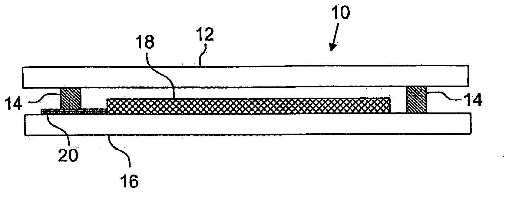
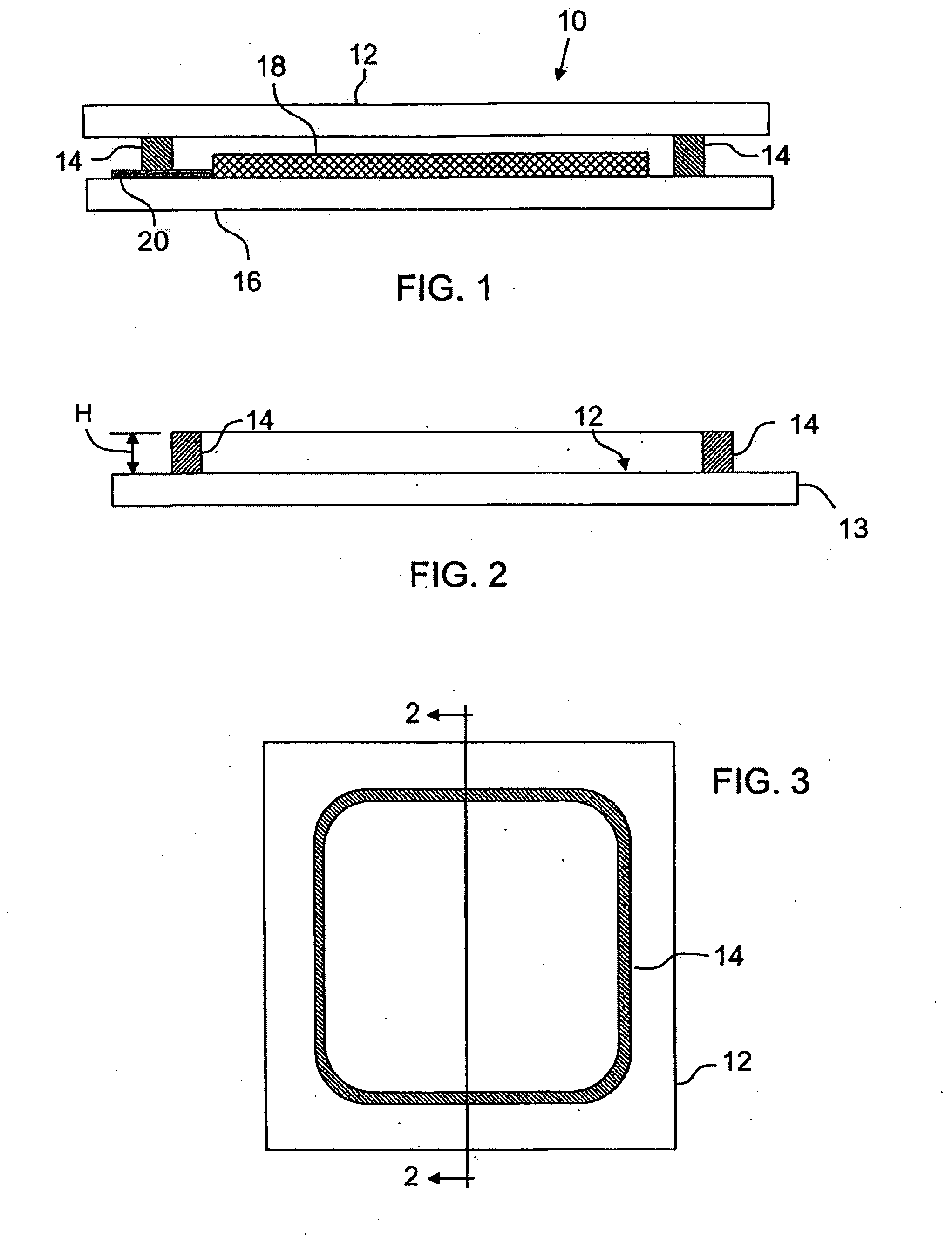
[0037]FIG. 1 is a schematic, cross-sectional, side view of a hermetically sealed OLED display device, generally designated by reference numeral 10, comprising a first substrate 12, a sintered frit pattern 14, a second substrate 16, at least one OLED element 18, and at least one electrode 20 in electrical contact with the OLED element. Typically, OLED element 18 is in electrical contact with an anode electrode and a cathode electrode. Electrode 20 in FIG. 1 is intended to represent either electrode. Although only a single OLED element is shown for simplicity, display device 10 may have many OLED elements disposed therein. The typical OLED element 18 includes one or...


PUM

PropertyMeasurementUnit
Lengthaaaaaaaaaa
Lengthaaaaaaaaaa
Lengthaaaaaaaaaa

Abstract

Packages for elements, e.g., OLEDs, that are temperature sensitive are provided. The packages have a first glass substrate (12), a second glass substrate (16), and a wall (14) that separates the first and second substrates (12,16) and hermetically seals at least one temperature sensitive element (18,28,36) between the substrates (12,16). The wall (14) comprises a sintered frit and at least a portion of the wall is laser sealed to the second substrate (16) by melting a glass component of the sintered frit. The minimum width (40) of the laser-sealed portion of the wall (14) at any location along the wall (14) is greater than or equal to 2 millimeters so as to provide greater hermeticity and strength to the package. The laser sealing is performed without substantially degrading the temperature sensitive element(s) (18,28,36) housed in the package.

Description

I. FIELD OF THE INVENTION[0001]This invention relates to methods and apparatus for packaging electronic components, such as the organic light emitting diodes (OLEDs) used in display devices.II. BACKGROUND OF THE INVENTION[0002]OLED-based displays are currently being considered for use in many applications which presently employ liquid crystal displays (LCDs). OLED-based displays can provide brighter and clearer images than liquid crystal displays and also need less power. However, OLEDs are susceptible to damage resulting from exposure to oxygen and moisture. Such exposure may lead to a reduction in the useful life of the light emitting device. Therefore, hermetic sealing is one of basic requirements for long term performance of OLEDs.[0003]Efforts have been made to hermetically seal OLED-based displays with organic materials, such as epoxy resins. An alternate technology with substantially better performance has been developed by Corning Incorporated, the assignee of this applicati...

Claims


Application Information

Patent Timeline
IPC IPC(8): H01L27/28H01J9/24H05B33/00C03C8/24
CPCH01L51/5237H10K59/8722H10K71/421H05B33/04H10K50/8426
Inventor LOGUNOV, STEPHAN LVOVICHLOREY, JOHN DAVIDSCHNEIDER, VICTOR MARINO
Owner CORNING INC
Learn More