Mobile phone
a technology for information communication devices and mobile phones, applied in static indicating devices, instruments, substation equipment, etc., can solve problems such as inability to optimize size or arrangement, complicated operation, and hamper convenience, and achieve the effect of improving operation
- Summary
- Abstract
- Description
- Claims
- Application Information
AI Technical Summary
Benefits of technology
Problems solved by technology
Method used
Image
Examples
embodiment mode 1
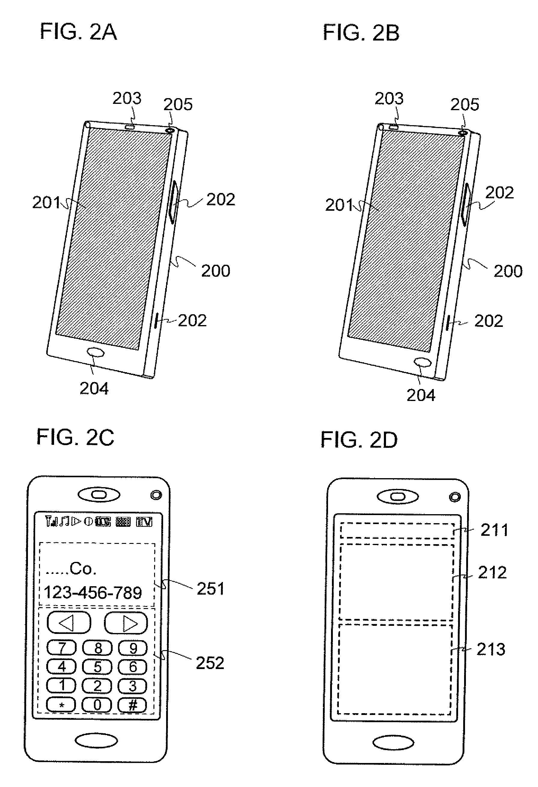
[0034]In this embodiment mode, the structures and functions of a mobile phone are described with reference to a block diagram and the like. Note that a mobile phone in this specification refers to a mobile information-communication device which has an image function of, for example, receiving television broadcasts to display images, a calling function using communication through base stations of the mobile phone, a function of transmitting and receiving e-mail or the like through the Internet, or the like. Note that the number of functions of a mobile phone may be plural, and the functions are not limited to the above functions.
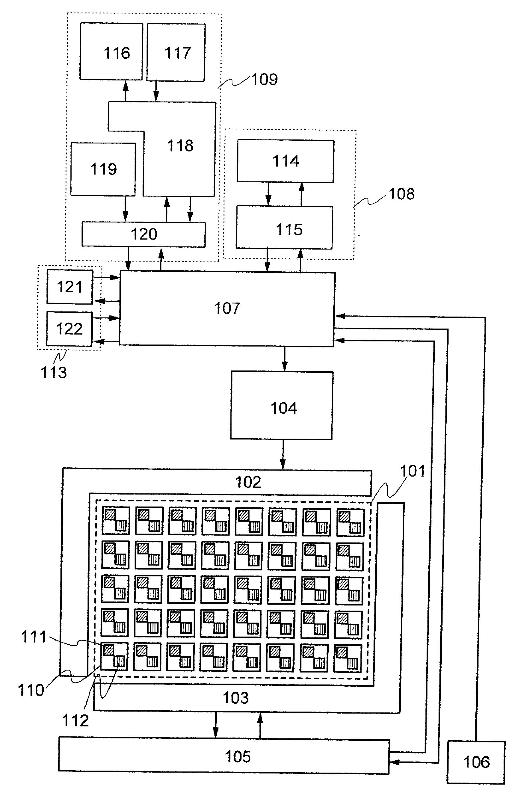
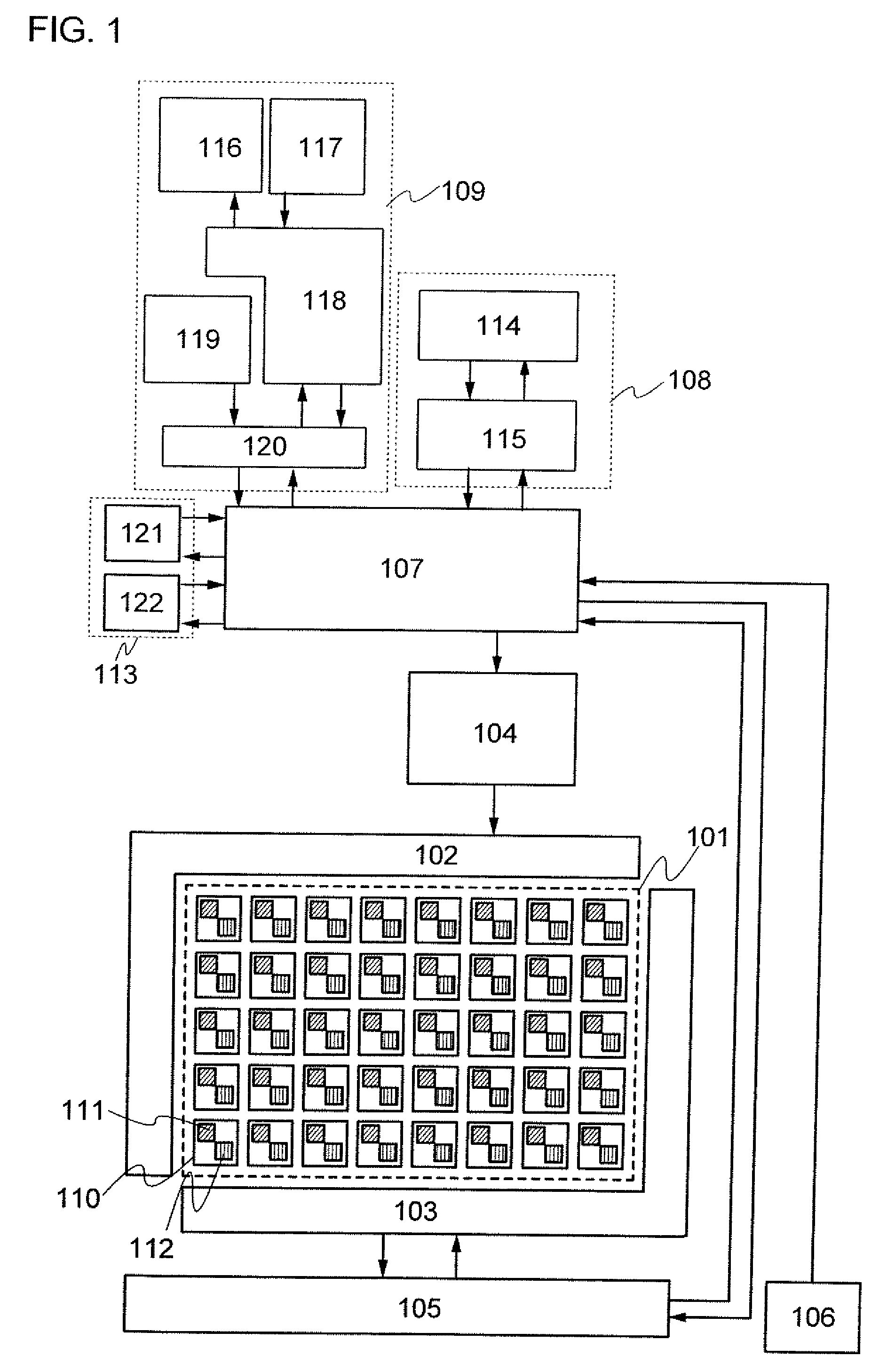
[0035]FIG. 1 is a block diagram of a mobile phone which is described in this embodiment mode. The mobile phone shown in FIG. 1 includes a pixel circuit portion 101, a display element driver circuit 102, an optical sensor driver circuit 103, a display portion control circuit 104, an optical sensor control circuit 105, a gradient detection portion 106, an arith...
embodiment mode 2
[0077]In this embodiment mode, examples of the structures of the pixel circuit portion 101, the display element driver circuit 102, and the optical sensor driver circuit 103 which are provided around the display portion of the mobile phone used in the present invention are described. FIG. 8 is a block diagram of the pixel circuit portion 101, the display element driver circuit 102, and the optical sensor driver circuit 103. In FIG. 8, the display element driver circuit 102 includes a data line driver circuit 320 and a scan line driver circuit 322. Further, the optical sensor driver circuit 103 includes an optical sensor signal line driver circuit 321 and an optical sensor scan line driver circuit 323 that control the driving of a reset transistor, a buffer transistor, and a selection transistor provided in each pixel.
[0078]The data line driver circuit 320 includes a shift register 320a, a latch (A) 320b, and a latch (B) 320c. In the data line driver circuit 320, a clock signal (CLK)...
embodiment mode 3
[0093]In this embodiment mode, a method for manufacturing each transistor included in the pixel circuit portion over a substrate having an insulating surface is described in detail. First, as shown in FIG. 10A, a first insulating film 702a and a second insulating film 702b are formed over a substrate 701. A first semiconductor layer 703, a second semiconductor layer 704, a third semiconductor layer 705, a fourth semiconductor layer 706, and a fifth semiconductor layer 707 are formed over the second insulating film 702b.
[0094]As the substrate 701, a glass substrate, a quartz substrate, a ceramic substrate, a plastic substrate, a semiconductor substrate, a sapphire substrate, a metal substrate, or the like can be used. The semiconductor layers can be formed using single crystal silicon, germanium, a compound semiconductor such as gallium arsenide or indium phosphide, or the like.
[0095]Further, the substrate 701 is attached to the first semiconductor layer 703, the second semiconducto...
PUM
 Abstract
Description
Claims
Application Information


