Stacked-type chip package structure and fabrication method thereof

a technology of chip package and fabrication method, which is applied in the direction of electrical equipment, semiconductor devices, semiconductor/solid-state device details, etc., can solve the problems of inconvenient fabrication of vias having a high aspect ratio on silicon substrates, increased number of memory chips, and inability to meet the requirements of the customer, so as to achieve satisfactory reworkability and flexibility, the effect of improving production efficiency and reliability of products

Active Publication Date: 2009-06-11
NAN YA TECH
View PDF9 Cites 25 Cited by
  • Summary
  • Abstract
  • Description
  • Claims
  • Application Information

AI Technical Summary

Benefits of technology

[0019]In the present invention, the flexible circuit boards having the conductive pillars are sequentially stacked on the conductive bumps, and each layer of the chip and each layer of the flexible circuit boards are electrically connected to each other through the same layer of the conductive wires. As such, the package structure with multi-layer chips is formed on the substrate. The fabrication of the conductive pillars on the flexible circuit boards does not pose a negative impact on the electrical performance and reliability of the integrated circuits in the chips. Moreover, production efficiency and reliability of the products can be improved by utilizing the flexible circuit boards characterized by satisfactory reworkability and flexibility.

Problems solved by technology

Nevertheless, due to a rising demand for the storage capacity of the memory module, the number of the memory chips increases accordingly, and additional area occupied by the circuit board is required.
Nevertheless, fabricating the vias having a high aspect ratio on the silicon substrate is not cost-effective, and is inferior to mass production.
Besides, when an arrangement of the solder balls 30 on the chips 10 follows the trend of fine pitch, the shortened distance between the solder balls 30 may give rise to an overflow of the solder balls 30 during a reflow process, which is likely to cause circuit shortage.
Moreover, the fabrication of the vias having a high aspect ratio on the silicon substrate negatively affects electrical performance and reliability of integrated circuits in the chips, thus poses an impact on the operation of the entire circuit system.

Method used


Image

  • Stacked-type chip package structure and fabrication method thereof
  • Stacked-type chip package structure and fabrication method thereof
  • Stacked-type chip package structure and fabrication method thereof

Examples


Embodiment Construction

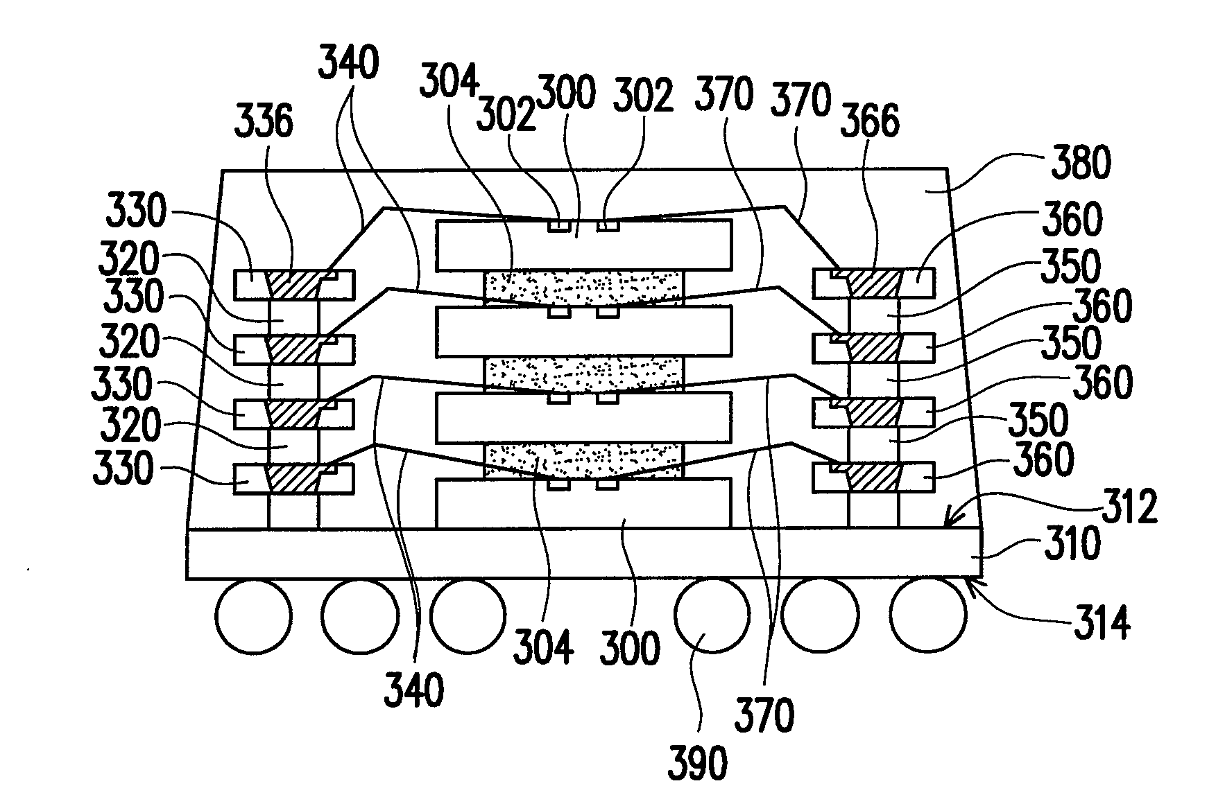
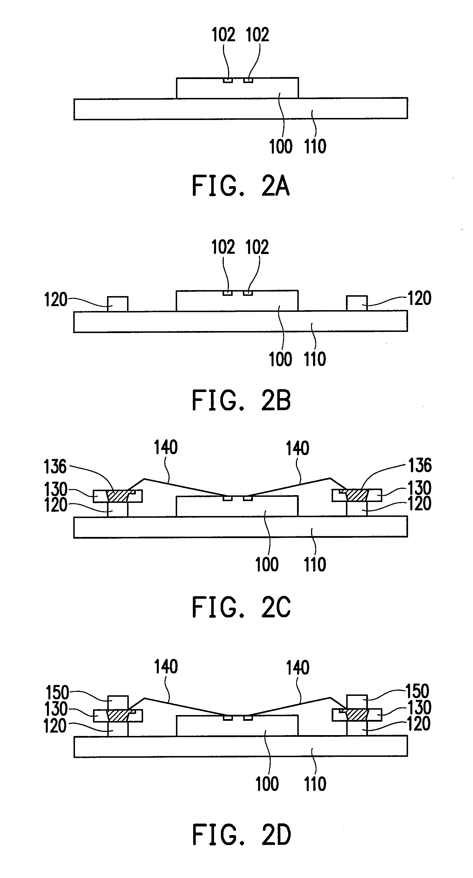
[0026]FIGS. 2A through 2H are schematic views illustrating steps of fabricating a stacked-type chip package structure according to an embodiment of the present invention. The steps are enumerated as follows:

[0027](a) disposing a first layer of a chip 100 on a substrate 110;

[0028](b) disposing a first layer of conductive bumps 120 on the substrate 110 by a stud-bump bonding process;

[0029](c) disposing a first layer of flexible circuit boards 130 on the first layer of the conductive bumps 120;

[0030](d) forming a first layer of conductive wires 140 between the first layer of the chip 100 and the first layer of each of the flexible circuit boards 130 by a wire bonding process to electrically connect the first layer of the chip 100 and the first layer of each of the flexible circuit boards 130;

[0031](e) disposing a second layer of conductive bumps 150 on the first layer of the flexible circuit boards 130 by the stud-bump bonding process;

[0032](f) disposing a first layer of a spacer layer...


PUM


Abstract

A stacked-type chip package structure in which stacked chips and stacked flexible circuit boards are disposed on a substrate. A plurality of spacer layers is respectively sandwiched between two adjacent chips and stacked on top of each other. In addition, conductive bumps are disposed on the substrate and between the stacked flexible circuit boards, such that the stacked flexible circuit boards are electrically connected to the substrate. Besides, conductive wires are electrically connected between the flexible circuit boards and the chips, so as to form a package structure with multi-layer chips on the substrate. Thereby, electrical performance and reliability of the chips are improved.

Description

CROSS-REFERENCE TO RELATED APPLICATION[0001]This application claims the priority benefit of Taiwan application serial no. 96146571, filed on Dec. 6, 2007. The entirety the above-mentioned patent application is hereby incorporated by reference herein and made a part of specification.BACKGROUND OF THE INVENTION[0002]1. Field of the Invention[0003]The present invention generally relates to a chip package structure, and in particular, to a stacked-type chip package structure and a fabrication method thereof.[0004]2. Description of Related Art[0005]A stacked-type chip package structure is a semiconductor package structure in which a three-dimensional package technology is employed to vertically stack a plurality of chips. The stacked-type chip package structure can be applied to storage devices such as memory modules, memory cards, portable flash disks, and so forth. The memory module normally applying to a desktop computer, a notebook computer, or an industrial computer is a standardize...

Claims


Application Information

Patent Timeline
Patent Type & Authority Applications(United States)
IPC IPC(8): H01L23/02
CPCH01L25/0657H01L2224/32145H01L2224/45144H01L2924/15311H01L2924/01079H01L2224/48091H01L2224/73265H01L2224/92247H01L2225/0651H01L2225/06527H01L2225/06575H01L2924/00014H01L2924/00
Inventor CHEN, JEN-CHUNYANG, WU-DER
Owner NAN YA TECH
Why Eureka
Try Eureka