Wafer-level burn-in method and wafer-level burn-in apparatus

a burn-in apparatus and wafer-level technology, applied in the direction of individual semiconductor device testing, semiconductor/solid-state device testing/measurement, instruments, etc., can solve the problems of insufficient screening, considerable damage, and the temperature of the wafer cannot be controlled to the desired temperature, so as to prevent the wear and burn of the probe. , the effect of high reliability

Inactive Publication Date: 2009-06-25
PANASONIC CORP
View PDF6 Cites 32 Cited by
  • Summary
  • Abstract
  • Description
  • Claims
  • Application Information

AI Technical Summary

Benefits of technology

[0015]In order to solve the problems, an object of the present invention is to provide a wafer-level burn-in method and a wafer-level burn-in apparatus with high reliability which can prevent the wear and burn of a probe by controlling the temperature of a wafer to a desired temperature, not depending upon the distribution of good devices formed on the wafer and the power consumptions of devices.

Problems solved by technology

Moreover, of devices formed on a wafer, an electrical load is not applied to devices judged as defective in upstream operations and thus heat is not generated by energization on the devices.
For these reasons, in some cases, a difference occurs between a temperature measured by the temperature sensor and an actual temperature and thus a wafer temperature cannot be controlled to a desired temperature.
Unfortunately, the wafer temperature increased by the temperature difference may cause considerable damage such as serious wear or burn on a probe for applying an electrical load to a wafer.
Further, a temperature decrease may disadvantageously cause insufficient screening using a thermal load and defective devices may be introduced onto the market.
Further, the power consumption is a design value.

Method used


Image

  • Wafer-level burn-in method and wafer-level burn-in apparatus
  • Wafer-level burn-in method and wafer-level burn-in apparatus
  • Wafer-level burn-in method and wafer-level burn-in apparatus

Examples


first embodiment

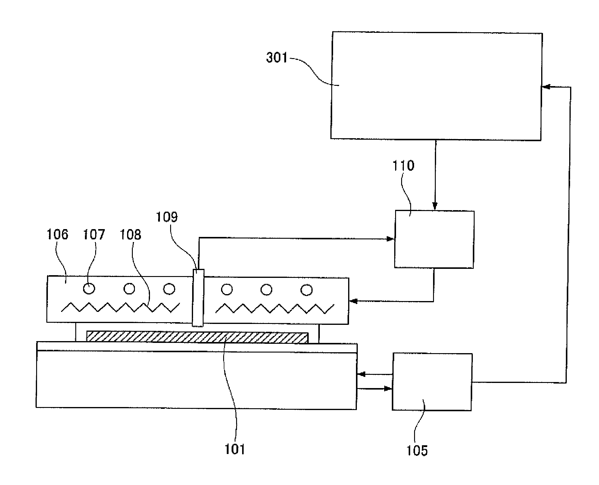
[0044]FIG. 1 is a schematic diagram showing a wafer-level burn-in apparatus according to a first embodiment of the present invention. In the first embodiment of FIG. 1, a temperature correction value calculator 301 is added to the configuration of FIG. 4.

[0045]In wafer-level burn-in using this configuration according to the first embodiment, when an electrical load is applied to devices formed on a wafer 101, a difference between the actual temperature of the wafer 101 heated by the power consumption of the devices and a temperature measured by a temperature sensor 109 is calculated beforehand by experiment as a calorific value per unit area of the wafer 101, that is, a heat density function. The first embodiment uses the following direct proportional relationship:

ΔT=γ×D  (1)

where ΔT represents a difference between the actual temperature of the wafer 101 and a temperature measured by the temperature sensor 109, D represents the heat density of good devices on the wafer 101, and γ re...

second embodiment

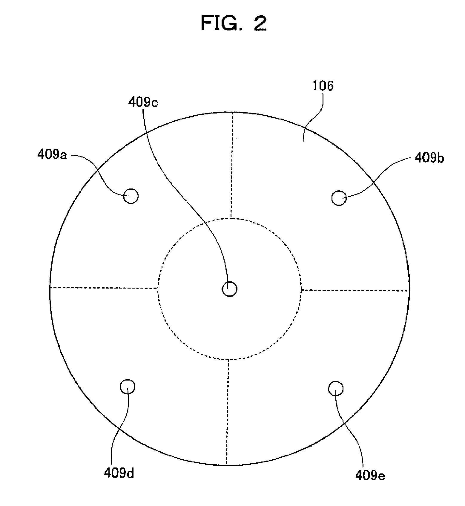
[0049]FIG. 2 is a schematic diagram showing a divided temperature regulating plate according to a second embodiment of the present invention. FIG. 6 is a schematic diagram showing a wafer-level burn-in apparatus according to the second embodiment.

[0050]In the second embodiment of the present invention, as shown in FIG. 2, a temperature regulating plate 106 in the configuration of FIG. 1 is divided into five areas of area “a” to “e”. As shown in FIG. 6, heaters 601, coolant passages 607, temperature sensors 409a to 409e, temperature regulators 610, and temperature correction value calculators 611 are independently disposed and temperature control is performed for each divided area. In other words, unlike the first embodiment for handling a measurement error caused by a heat density, the second embodiment also handles variations in heat density in the respective areas of a wafer.

[0051]In wafer-level burn-in according to the second embodiment configured thus, when an electrical load is...

third embodiment

[0056]A third embodiment of the present invention is configured like the first embodiment of FIG. 1.

[0057]In wafer-level burn-in according to the third embodiment, regarding a difference between a temperature measured by a temperature sensor 109 and the actual temperature of a wafer 101 during heat generation on devices by power consumption, the influence varies with a distance between the temperature sensor 109 and the devices formed on the wafer 101. Considering this point, a weight constant is set for each device according to a distance in the planar direction of the wafer 101 from the temperature sensor 109 based on the relationship between the temperatures of the temperature sensor 109 and the wafer 101 in each thermal distribution and at each heat density, through experiment in which the temperature sensor is installed beforehand and a wafer allowing heat generation with a desired thermal distribution and a desired heat density is used. In other words, unlike the first embodim...


PUM


Abstract

Temperature control in wafer-level burn-in is performed such that a set temperature used for the temperature control is corrected using a correction value calculated from the generated heat density of a wafer (101). Thus it is possible to eliminate a difference between the temperature of the wafer heated when an electrical load is applied and a control temperature for applying a thermal load, not depending on the distribution of good devices formed on the wafer (101) and the power consumption of the devices. As a result, the wear and burn of a probe can be prevented and highly reliable screening can be achieved.

Description

TECHNICAL FIELD[0001]The present invention relates to a wafer-level burn-in method and a wafer-level burn-in apparatus which perform screening by applying an electrical load and a thermal load to a semiconductor wafer.BACKGROUND ART[0002]Conventionally, in screening test apparatuses generally called burn-in apparatuses, defective pieces are screened by conducting power-on tests in thermal atmospheres at predetermined temperatures (e.g., 125° C.) to distinguish potential defects, after the packaging of IC chips having been obtained by dividing a semiconductor wafer.[0003]Such a conventional apparatus requires a large thermostat and a large calorific value and thus has to be separated from other manufacturing lines. It has been desired to conduct burn-in tests on wafers before dividing the wafers into chips because wafers has to be transported, mounted in an apparatus, and loaded and unloaded into and from the apparatus, defective pieces found after packaging cause excessive packaging...

Claims


Application Information

Patent Timeline
Patent Type & Authority Applications(United States)
IPC IPC(8): G01R31/02
CPCH01L21/67248G01R31/2874G01R31/26H01L22/00
Inventor SEGAWA, TERUTSUGUSANADA, MINORU
Owner PANASONIC CORP
Why Eureka
Try Eureka