Inspection apparatus and inspection method

a technology of inspection apparatus and inspection method, applied in the direction of optical radiation measurement, 2d-image generation, instruments, etc., to achieve the effect of improving the sensitivity of inspection

Inactive Publication Date: 2009-06-25
HITACHI HIGH-TECH CORP
View PDF13 Cites 36 Cited by
  • Summary
  • Abstract
  • Description
  • Claims
  • Application Information

AI Technical Summary

Benefits of technology

[0030]According to the invention, a defect inspection method and apparatus having improved sensitivity of an inspection on a short-circuit at the bottom between neighboring wires and capable of detecting even a pattern short-circuit at the bottom between a plurality of wires arranged in parallel in a finely formed pattern can be realized.

Problems solved by technology

To shorten the time of setting a threshold, it is a problem to efficiently find a false defect from defect candidates and to obtain a threshold with which false defects can be deleted by the smallest number of review times.

Method used


Image

  • Inspection apparatus and inspection method
  • Inspection apparatus and inspection method
  • Inspection apparatus and inspection method

Examples


second embodiment

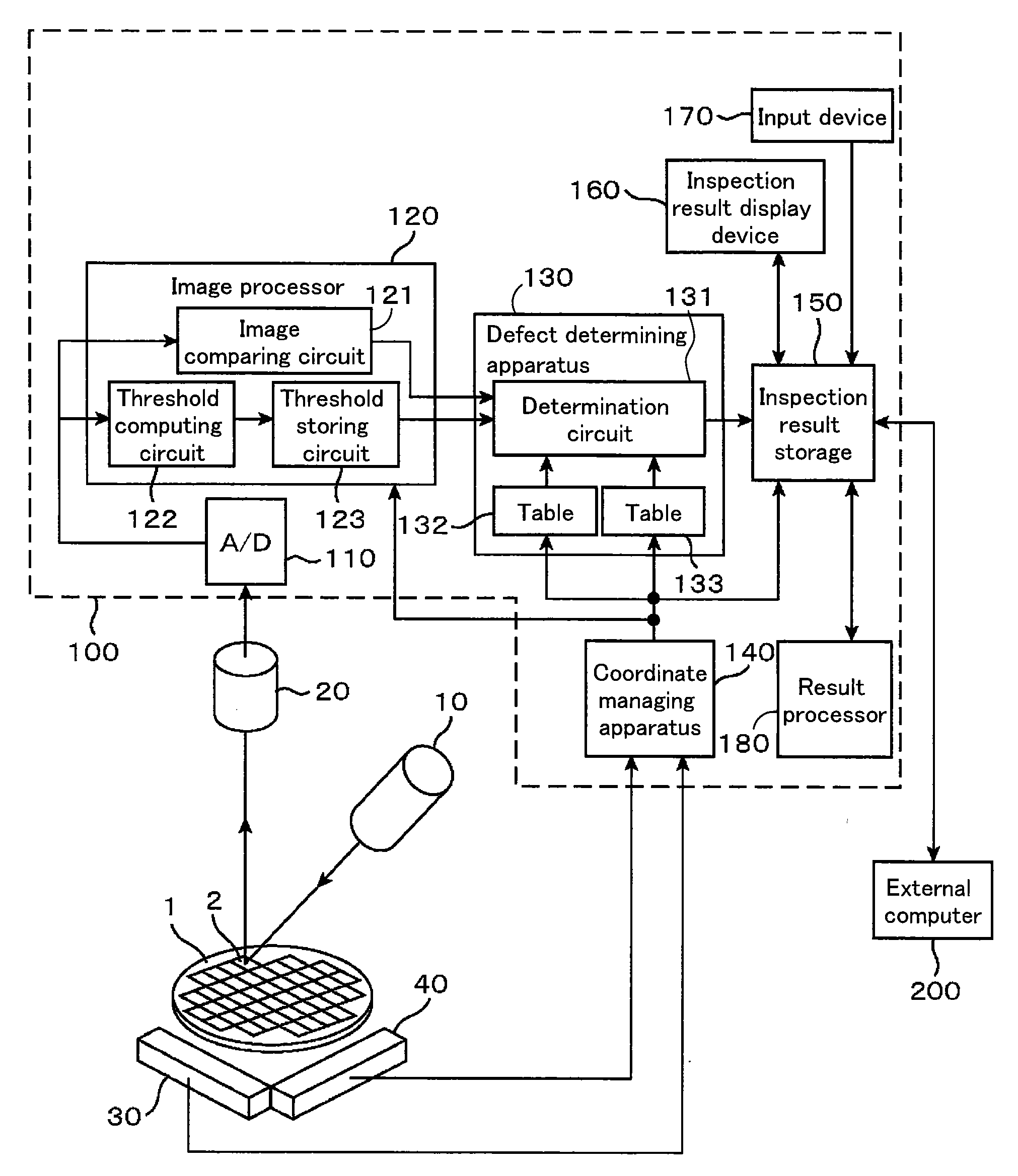
[0142]FIG. 8 is a general schematic configuration diagram of a defect inspection apparatus to which the invention is applied. In FIG. 8, a sample 801 (a semiconductor wafer, a display device, a printed board, or the like) as an object to be inspected is mounted on a stage 815. The stage 815 is, for example, a combination of an XY stage, a Z stage, a θ stage, and the like.

[0143]An apparatus capable of scanning the sample 801 in the XY plane is employed so that the entire surface of the sample 801 can be inspected by inspection optical systems 804 and 805 disposed above the stage 815. The sample 801 is irradiated with illumination light 802 emitted from an illumination optical system 803 (including a light source). Light incident on the inspection optical systems 804 and 805 disposed above the sample 801, of scattered reflection light from a defect such as a pattern, a particle, and the like on the sample 801 is led to sensors 806 and 807, photoelectrically converted, and transmitted ...

third embodiment

[0171]FIGS. 13A and 13B are schematic configuration diagrams of the illumination optical system 803 of the defect inspection apparatus in a third embodiment of the invention. Since the general configuration of the defect inspection apparatus is similar to that of the example shown in FIG. 8, it will not be shown and its description will not be repeated.

[0172]In FIGS. 13A and 13B, a beam (coherent light) of illumination light of linearly-polarized light or elliptically-polarized light emitted from a light source 300 passes through a depolarizer 310, and is expanded by a beam expander 320. The expanded beam enters multiple glass block element 330. The light passed through the multiple glass block element 330 is condensed on a straight line by a cylindrical lens 340, and the condensed light reaches the illumination region 325 on the surface of the sample 801.

[0173]As the depolarizer 310, for example, a birefringent substrate made of crystal or the like which is processed in a wedge for...

fourth embodiment

[0181]FIGS. 14A and 14B are schematic configuration diagrams of the illumination optical system 803 of the defect inspection apparatus in a fourth embodiment of the invention. Since the general configuration of the defect inspection apparatus is similar to that of the example shown in FIG. 8, it will not be shown and its description will not be repeated.

[0182]In the fourth embodiment of the invention, a beam of illumination light of linearly-polarized light or elliptically-polarized light emitted from the light source 300 passes through a half-wavelength plate 350 and is expanded by the beam expander 320. The expanded beam passes through a half-wavelength plate 360 provided in a region of about the half of the aperture. The beam passed through the half-wavelength plate 360 is incident on multiple glass block element 370. The beam passed through the multiple glass block element 370 is condensed on a straight line by the cylindrical lens 340, and the condensed light reaches the illumi...


PUM

PropertyMeasurementUnit
thresholdaaaaaaaaaa
frequencyaaaaaaaaaa
defect inspectionaaaaaaaaaa

Abstract

The invention is directed to find a false defect from defect candidates and obtain a threshold with which the false defect can be eliminated by the smallest number of review times. Defect candidates are reviewed and selected as a defect or a false defect. By deleting a defect candidate having a characteristic quantity equal to or less than that of the false defect from a map or displaying it in another sign, the false defect can be determined visually. Since the defect candidate having the characteristic quantity equal to or less than that of the selected false defect is deleted from the map or displayed in another sign, the defect candidates unnecessary to set a threshold are not reviewed. The number of defect candidates to be reviewed can be largely reduced as compared with that in the conventional technique. Further, by repeating the above work, the threshold is automatically calculated, and an inspection result map with the threshold is displayed, so that a re-inspection is unnecessary.

Description

BACKGROUND OF THE INVENTION[0001]1. Field of the Invention[0002]The invention relates to an inspection apparatus and an inspection method for detecting particles, flaw, defect, dirt, and the like (hereinbelow, generically called defect) existing in the surface of an object to be inspected such as a semiconductor wafer.[0003]The invention relates to a defect inspection method and a defect inspection apparatus for detecting a defect such as a particle or deformation in a pattern in a manufacturing process of a semiconductor device, a liquid crystal display device, a printed board, or the like.[0004]2. Description of the Related Art[0005]For example, an inspection apparatus for detecting a defect in a semiconductor wafer detects a defect existing in the surface of a wafer by irradiating the surface of the wafer with inspection light such as a laser beam and detecting reflection light or scattered light generated on the surface of the wafer.[0006]In the inspection apparatus of this kind...

Claims


Application Information

Patent Timeline
Patent Type & Authority Applications(United States)
IPC IPC(8): G01N21/88G06T11/20G06K9/00G06V10/145
CPCG01N21/9501G01N21/956G01N21/95607G01N2021/8848G01N21/88G06K9/2036G06K2209/19G06T7/00G01N2021/8861G06V10/145G06V2201/06
Inventor YAMASHITA, HIROYUKISAKAIYA, NORIOSHIMURA, KEIITO, MASAAKI
Owner HITACHI HIGH-TECH CORP
Why Eureka
Try Eureka