Defect inspection method and apparatus therefor

Active Publication Date: 2012-04-19
HITACHI HIGH-TECH CORP
View PDF4 Cites 38 Cited by
  • Summary
  • Abstract
  • Description
  • Claims
  • Application Information

AI Technical Summary

Benefits of technology

[0017]According to an aspect of the present invention, it is possible to improve inspection sensitivity using images under plural p

Problems solved by technology

Since the size of defects or foreign substances that are objects for detection becomes thus smaller, reflected, diffracted, and scattered light from these defects and foreign substances are really weak, and it is difficult to optically detect them.
However, there is no specific description to obtain two responses.
There are problems in that the distributions of r

Method used


Image

  • Defect inspection method and apparatus therefor
  • Defect inspection method and apparatus therefor
  • Defect inspection method and apparatus therefor

Examples


first embodiment

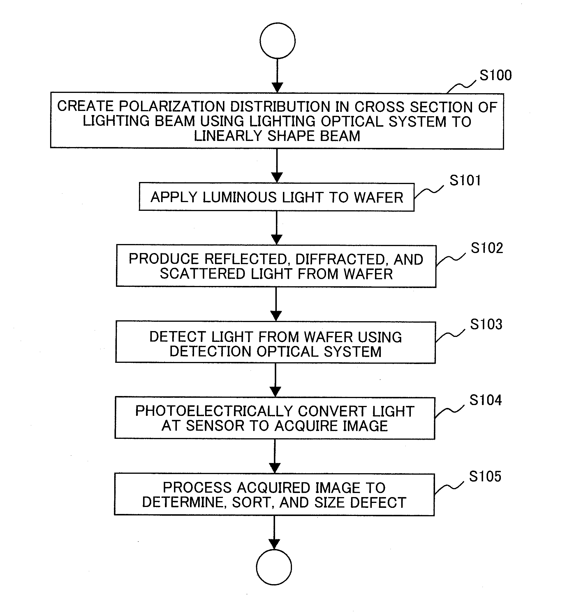
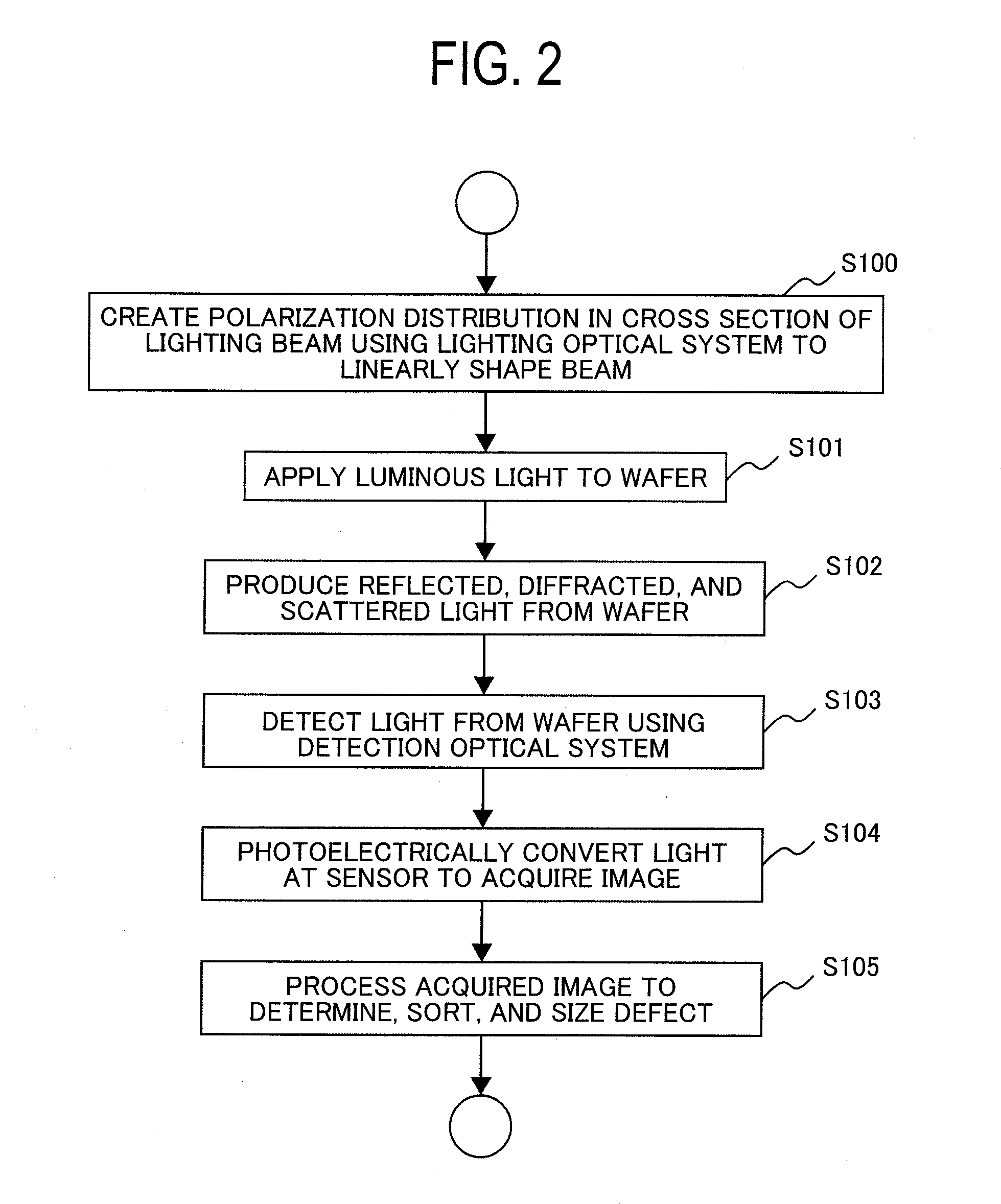
[0047]A first embodiment of the present invention will be described with reference to FIGS. 1 to 7. In the following, inspection performed by a dark field inspection apparatus for a semiconductor wafer will be described as an example.

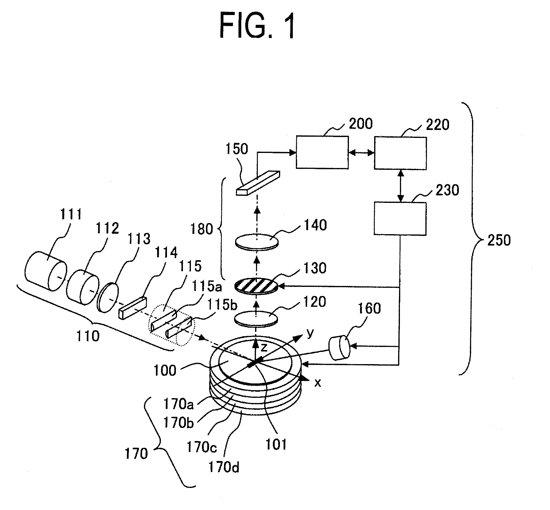
[0048]FIG. 1 shows the outline of the configuration of an optical dark field inspection apparatus. The dark field inspection apparatus according to this embodiment is mainly configured of a lighting optical system 110, a stage unit 170, a detection optical system 180, and a signal processing and control system 250. The lighting optical system 110 includes a light source 111, a beam shaper 112, a polarization control device 113 formed of a polarizer or a wave plate, a polarization control device array 114 that provides a distribution of polarization of light in a cross section of a beam, and a lens 115 that images the polarization distributed light in the cross section of the beam on an inspection object (a semiconductor wafer). The stage unit 170 is con...

second embodiment

[0068]A second embodiment of the present invention will be described with reference to FIGS. 8A and 8B and FIG. 9. An optical system according to the second embodiment of the present invention is different from the optical system according to the first embodiment shown in FIG. 1 in the polarization control device array 114, the sensor array 150, and the image processor 200. In the following, differences from the first embodiment will be described.

[0069]In this embodiment, a polarization control device array 114c produces four kinds of states of polarization in a luminous light beam, and a sensor array 150 individually detects four kinds of polarization components of scattered light from polarized lights for each of four kinds of states of polarization, 16 kinds of images in total. The states of polarization can be expressed by three parameters in total, two linearly polarized light components having orientations orthogonal to each other and different at an angle of 45 degrees and a ...

third embodiment

[0077]A third embodiment of the present invention will be described with reference to FIG. 11.

[0078]FIG. 11 shows an optical system according to the third embodiment of the present invention. The third embodiment is different from the first embodiment in that there are two beams of luminous light. The system includes a light source 1111, a mirror 1117 that diverges the optical path of a laser beam emitted from the light source 1111 to two lighting optical systems 1110 and 1120, in which a semiconductor wafer 100 is obliquely illuminated by using two luminous light beams 1121a and 1121b, and a detection optical system 1180 having an objective lens 1120 and an image forming lens 1140 to image reflected, diffracted, and scattered light of the luminous light beam 1121a from the illuminated semiconductor wafer 100 on the detection surface of a line sensor 1150x and to image reflected, diffracted, and scattered light of the luminous light beam 1121b on the detection surface of a line sens...


PUM


Abstract

To effectively utilize the polarization property of an inspection subject for obtaining higher inspection sensitivity, for the polarization of lighting, it is necessary to observe differences in the reflection, diffraction, and scattered light from the inspection subject because of polarization by applying light having the same elevation angle and wavelength in the same direction but different polarization. According to conventional techniques, a plurality of measurements by changing polarizations is required to cause a prolonged inspection time period that is an important specification of inspection apparatuses. In this invention, a plurality of polarization states are modulated in micro areas in the lighting beam cross section, images under a plurality of polarized lighting conditions are collectively acquired by separately and simultaneously forming the scattered light from the individual micro areas in the individual pixels of a sensor, whereby inspection sensitivity and sorting and sizing accuracy are improved without reducing throughput.

Description

BACKGROUND OF THE INVENTION[0001]The present invention relates to an inspection method for foreign substances or defects produced in fabricating an LSI and a liquid crystal substrate and an apparatus therefor.[0002]With the downscaling of semiconductor devices, the size of defects or foreign substances on a fine pattern that is an inspection object is a few nanometers or less. Since the size of defects or foreign substances that are objects for detection becomes thus smaller, reflected, diffracted, and scattered light from these defects and foreign substances are really weak, and it is difficult to optically detect them. Thus, such a method is proposed in which plural images are acquired under pluralities of lighting conditions and detection conditions (detection orientation, detection elevation angles, and polarization detection) and these images are used to improve defect detection sensitivity, using the fact that reflected, diffracted, and scattered light from defects or foreign ...

Claims


Application Information

Patent Timeline
IPC IPC(8): H04N7/18
CPCG01N21/956G01N21/9501
Inventor TANIGUCHI, ATSUSHISHIBATA, YUKIHIROUENO, TAKETONAKATA, TOSHIHIKO
Owner HITACHI HIGH-TECH CORP
Why Eureka
Try Eureka