Optical inspection method and optical inspection apparatus

a technology of optical inspection and optical inspection apparatus, which is applied in the direction of instruments, originals for photomechanical treatment, semiconductor/solid-state device testing/measurement, etc., can solve the problems of increasing the risk of thermal damage to the sample, the wavelength of the available light source having an output suitable for detecting a contaminant particle or defect is limited, and cannot be shortened to less than a certain limit, so as to improve the detection sensitivity of contaminant particles or defects, the time required for inspection

Inactive Publication Date: 2008-01-03
HITACHI HIGH-TECH CORP
View PDF2 Cites 12 Cited by
  • Summary
  • Abstract
  • Description
  • Claims
  • Application Information

AI Technical Summary

Benefits of technology

[0008] In view of this situation, the object of this invention is to provide an optical inspection method and an optical inspection apparatus in which the detection sensitivity of contaminant particles or defects is improved without sacrificing the time required to inspect the whole surface of the sample, the time required for inspection of the whole surface of the sample is reduced without sacrificing the detection sensitivity of contaminant particles or defects, and both the detection sensitivity of contaminant particles or defects and the time required for inspection of the whole surface of the sample are improved. This invention is intended to provide a technique for achieving this object.
[0009] In order to achieve the object described above, according to this invention, there is provided an optical inspection apparatus comprising a means for forming not one but a plurality of illumination spots by radiating the illumination beam on the surface of the sample in order to generate and detect the scattered light from a contaminant particle or a defect on the sample surface and detecting by isolating the scattered light signal generated from the plurality of the illumination spots for each scattered light generated from each illumination spot. More specifically, there is provided an optical inspection apparatus comprising a sample stage for moving a sample in accordance with a predetermined pattern, an illumination means for radiating the light from a light source on the surface of the sample, and a light detection means for detecting the light generated by the radiation of the illumination beam on the sample, wherein the illumination means includes a means for splitting a single light flux generated from the light source into a plurality of light fluxes and forming a plurality of illumination spots in such a manner as to superpose at least a part of the loci plotted by the illumination spots generated in predetermined spaced relation with each other on the sample by the illumination means radiating the plurality of split light fluxes during the movement of the sample on the sample stage, and an optical signal isolation / detection means for detecting by isolating the signal detected at different time points by the light detection means from the light generated at the same position on the sample from the plurality of the illumination spots. There is also provided an optical inspection method implemented by the aforementioned optical inspection apparatus. The light source may be either a CW light source or a pulse light source for radiating the light intermittently. To facilitate the timing adjustment for synthesizing the detected light, however, the pulse light source is more preferable. This is by reason of the fact that the optical signal generated with the passage of the same position of the sample through the plurality of illumination spots is obtained from the photodetector, and the light emission timing of the pulse light emission can be used as a timing signal to synthesize the information for the same position. In the case of the CW light source, the timing signal for synthesis can be calculated based on the speed of the sample stage. In this method, the same point on the sample is inspected twice, and therefore, the inspection sensitivity can be improved. Also, the areas irradiated with the plurality of illumination spots on the sample are arranged not to be superposed one on another with the movement of the sample stage thereby to improve the throughput. Also in this case, the light emission timing of the pulse laser can be used to separate the optical signal information from the plurality of illumination spots. The layout patterns of the plurality of illumination spots can be large in number as described in the embodiment later, and each layout pattern can produce a unique effect. The photodetector is preferably a photomultiplier tube having a high response speed. Depending on the moving speed of the sample stage, however, an ordinary optical element such as a CCD can be used.
[0010] According to this invention, the detection sensitivity of contaminant particles or defects can be improved without sacrificing the time required for inspecting the whole surface of the sample, or the time required for inspecting the whole surface of the sample can be improved without sacrificing the detection sensitivity of contaminant particles or defects. Further, both the detection sensitivity of contaminant particles and defects and the time required for inspecting the whole surface of the sample can be improved at the same time.

Problems solved by technology

Under the circumstances, however, it is not easy to improve the sensitivity even if these measures are taken, for the reasons described below.
(1) An increased illuminance of the illumination beam causes the surface of the sample to absorb the energy of the illumination beam and increases the surface temperature of the sample thereby increasing the risk of thermal damage to the sample.
(2) The wavelength of the available light source having an output suitable for detecting a contaminant particle or defect is limited and cannot be shortened to less than a certain limit.
(4) In the prior art, the quantum efficiency and S / N of the photomultiplier tube used as a photodetector suitable for detecting weak scattered light have almost reached a theoretical limit and a further improvement thereof is not expected.
(6) A lower primary scanning rate, like in (5), leads to the disadvantage of a longer time required to inspect the whole surface of the sample.
(7) The mere increase in the diameter of the illumination spot along the primary scanning direction is not effective as it is offset by the increased background scattering due to the increased area of the illumination spot, while a decreased diameter of the illumination spot along the direction orthogonal to the primary scanning direction to prevent the illumination spot area from increasing, on the other hand, like in (5), disadvantageously lengthens the time required for inspection of the whole surface of the sample.

Method used


Image

  • Optical inspection method and optical inspection apparatus
  • Optical inspection method and optical inspection apparatus
  • Optical inspection method and optical inspection apparatus

Examples


Embodiment Construction

[0025] This invention is explained in detail below.

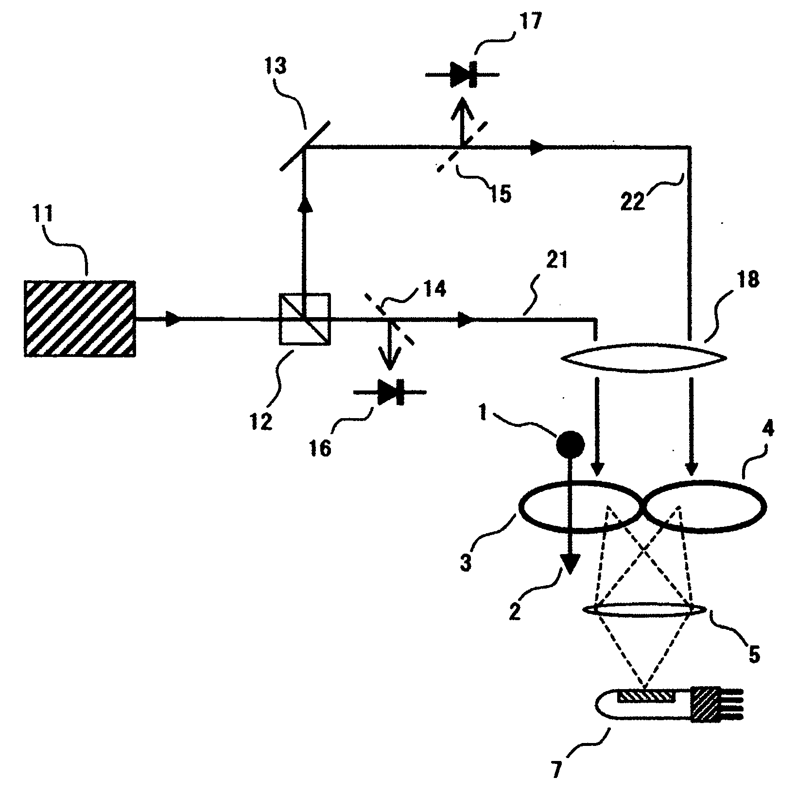
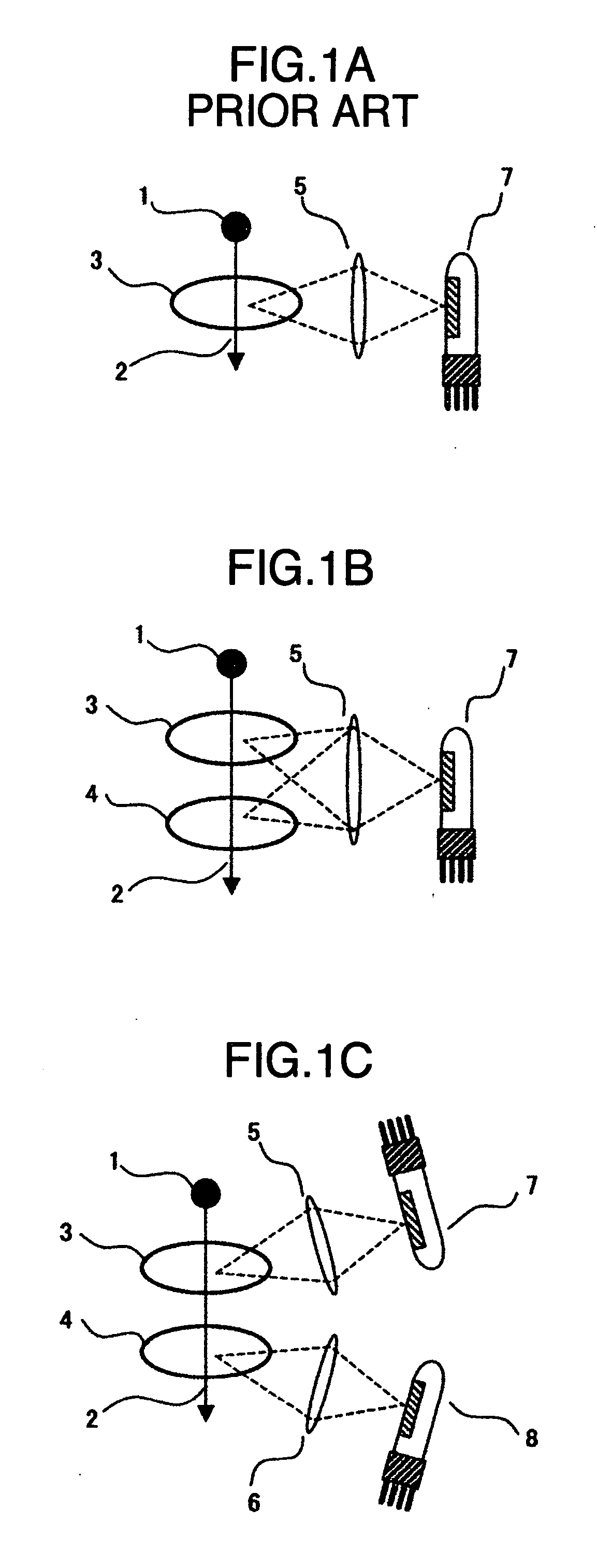
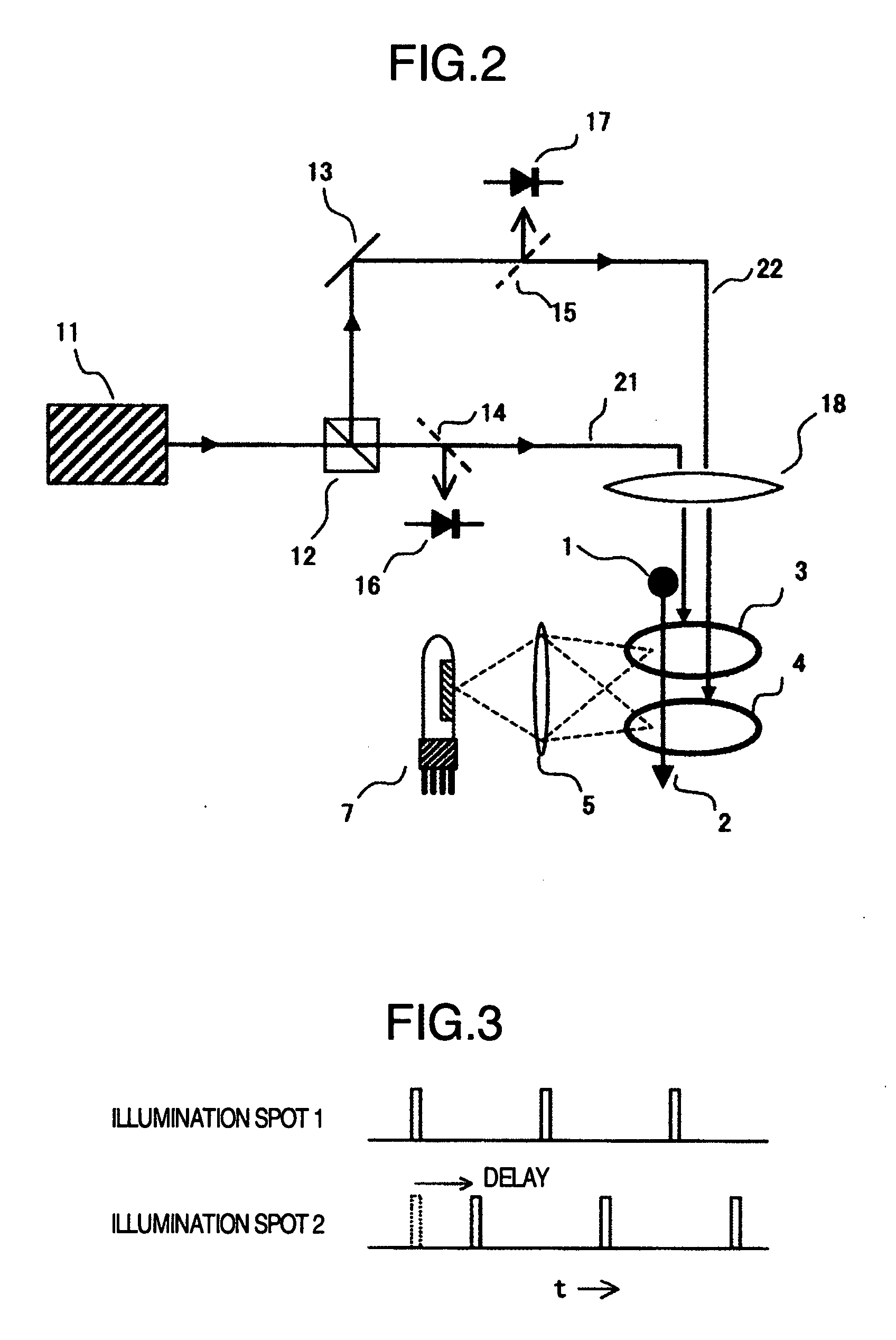
[0026] The configuration in which the scattered light generated from a single illumination spot is detected by a single photodetector as in the prior art is shown in FIG. 1A. A sample is mounted on a sample stage. The sample stage moves in a combination of a translation movement for primary scanning and another translation movement in the direction orthogonal to the first translation for secondary scanning or a combination of the rotational movement for primary scanning and the translation movement for secondary scanning. A contaminant particle 1 on the surface of the sample is moved along a locus 2 by the primary scanning of the sample stage. The contaminant particle 1, upon passage through an illumination spot 3 on the locus 2, generates the scattered light by the radiated light. This scattered light is condensed by a scattered light condenser lens 5, and detected and converted into a scattered light signal by a photodetector 7. ...


PUM

PropertyMeasurementUnit
optical path lengthaaaaaaaaaa
optical inspectionaaaaaaaaaa
elevationaaaaaaaaaa

Abstract

In the conventional contaminant particle/defect inspection method, if the illuminance of the illumination beam is held at not more than a predetermined upper limit value not to give thermal damage to the sample, the detection sensitivity and the inspection speed being in the tradeoff relation with each other, it is very difficult to improve one of the detection sensitivity and the inspection speed without sacrificing the other or improve both at the same time. The invention provides an improved optical inspection method and an improved optical inspection apparatus, in which a pulse laser is used as a light source, and a laser beam flux is split into a plurality of laser beam fluxes which are given different time delay to form a plurality of illumination spots. The scattered light signal from each illumination spot is isolated and detected by using a light emission start timing signal for each illumination spot.

Description

BACKGROUND OF THE INVENTION [0001] This invention relates to an optical inspection method and an optical inspection apparatus for detecting a contaminant particle or a defect of a sample to be inspected, such as a thin film substrate, a semiconductor substrate or a photomask by radiating light thereon, or in particular to an optical inspection method and an optical inspection apparatus having a sensitivity or a throughput improved as compared with the conventional method and apparatus. [0002] In the production line of a semiconductor substrate or a thin film substrate, the inspection is conducted for contaminant particles attached on the surface of the semiconductor substrate or the thin film substrate to monitor the dust generation in the manufacturing equipment. In the semiconductor substrate before forming a circuit pattern, for example, the detection of fine contaminant particles or micro defects on the order of not more than several tens of nm on the surface thereof is required...

Claims


Application Information

Patent Timeline
Patent Type & Authority Applications(United States)
IPC IPC(8): G01N21/88G01N21/956G03F1/84H01L21/027H01L21/66
CPCG01N21/9501G01N21/94
Inventor MATSUI, SHIGERU
Owner HITACHI HIGH-TECH CORP
Why Eureka
Try Eureka