Method and apparatus for inspecting defects

a technology of defect inspection and inspection method, applied in the direction of photomechanical apparatus, material analysis by optical means, instruments, etc., can solve the problems of scattered light, extremely small scattering light, and hardly obtained scattering light from defects, so as to suppress the lowering of the aperture ratio of the detection optical system, improve the capture ratio of defects, and improve the effect of inspection sensitivity

Active Publication Date: 2009-11-12
HITACHI HIGH-TECH CORP
View PDF6 Cites 36 Cited by
  • Summary
  • Abstract
  • Description
  • Claims
  • Application Information

AI Technical Summary

Benefits of technology

[0015]According to the present invention, it is possible to improve a capture ratio of defects by stably detecting scattered light to be detected that varies according to a shape, a structure, and a material of the defect with an illumination of a plurality of wavelengths.
[0016]Moreover, also in the case of the illumination with lights of a plurality of wavelengths, inspection sensitivity is improved by shielding the diffracted light of a normal pattern while suppressing lowering of an aperture ratio of a detection optical system and thereby detecting the scattered light of minute defects efficiently.
[0017]Further, in the case where the polarization state of scattered light differs from others depending on a defect kind, it is possible to improve the capture ratio of defects by performing spatial filtering without shielding the scattered light of the defect.

Problems solved by technology

However, with the light of the single wavelength, there is the case where the scattered light can hardly be obtained from the defect depending on optical constants of a defective material and the shape and structure around the defect.
As one example, although a silicon oxide film is used as an electric insulation film of the patterns that are stacked, an optically transparent oxide film generates thin film interference; therefore the intensity of the scattered light will vary depending on its film thickness.
Because of this phenomenon, the scattered light becomes extremely small with a film thickness condition of weakening light rays and becomes undetectable.
Since this leads to lowering of substantial resolution, there is a problem to be solved that contrast of a minute defect decreases and defect detection sensitivity lowers.
Therefore, if the scattered is filtered so as to become a linearly polarized light one the object side (wafer side) of the liquid crystal, in the case where the defect scattered light is polarized in a direction perpendicular to a filter transmission axis, the scattered light of the defect will be shielded and accordingly it will become impossible to detect the defect.

Method used


Image

  • Method and apparatus for inspecting defects
  • Method and apparatus for inspecting defects
  • Method and apparatus for inspecting defects

Examples


first embodiment

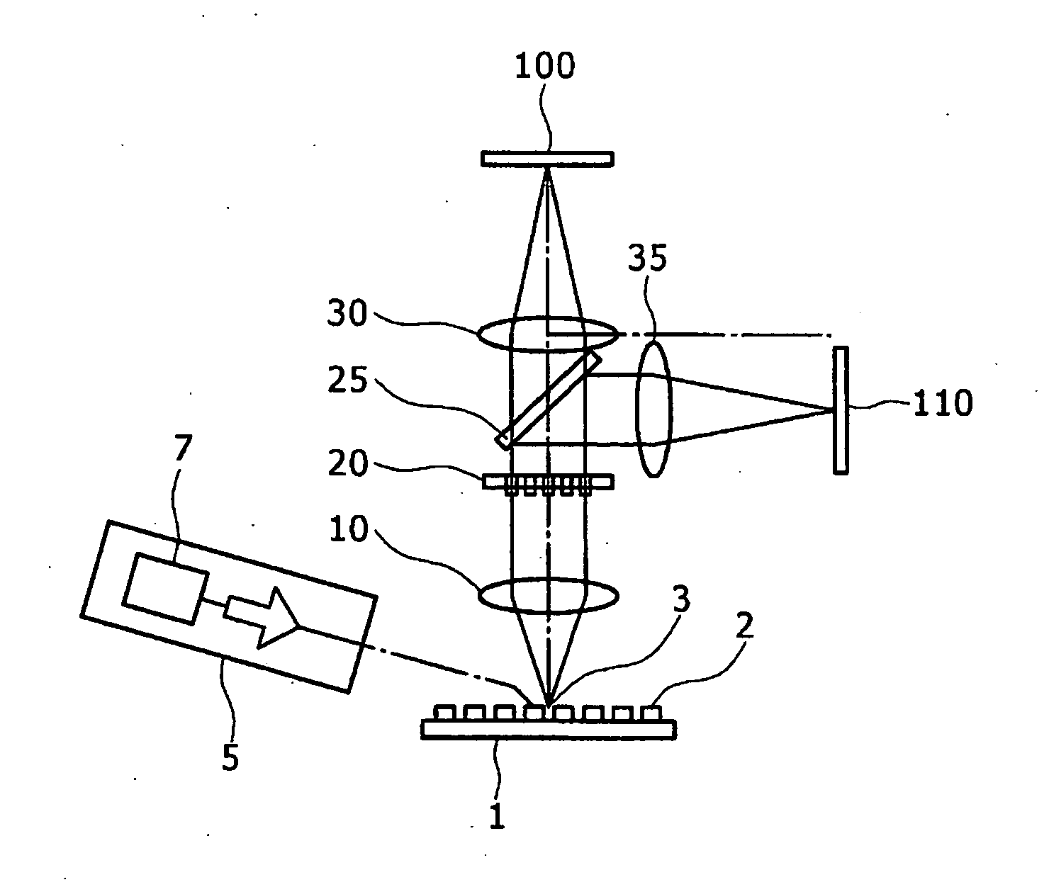
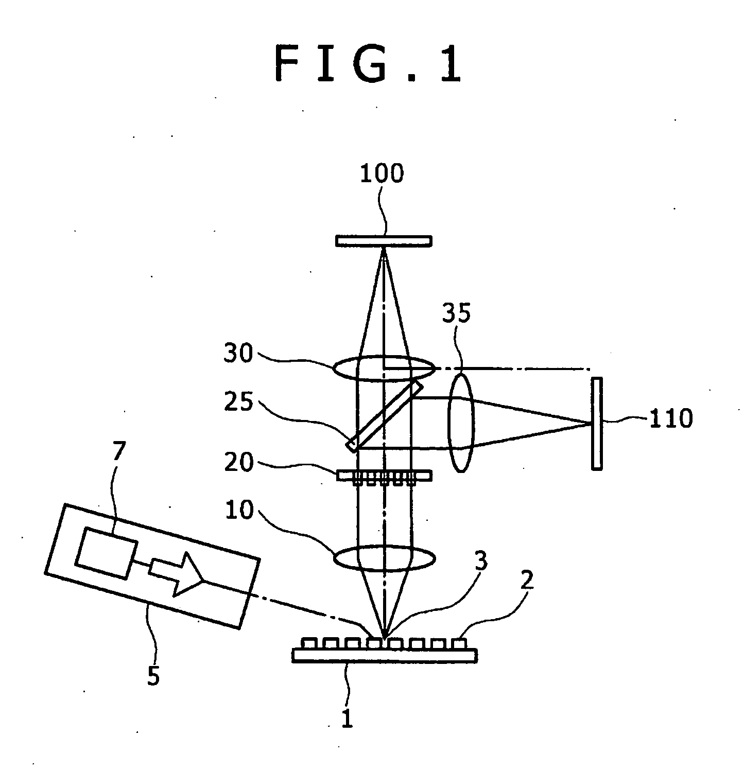
[0053]FIG. 1 shows a configuration of an apparatus for detecting defects of a specimen according to the present invention. A pattern 2 is formed on a wafer 1 and a defect 3 exists on the pattern 2. The wafer 1 is illuminated by an illumination optical system 5 of a plurality of wavelengths (in this embodiment, two wavelengths λ1, λ2) that is disposed slantingly relative to the wafer 1. For a light source 7 used in an illumination optical system 5, lights ranging from DUV (Deep Ultraviolet) lights to the visible lights such as: mercury lamps emitting the d line (588 nm), the e line (546 nm), the g line (436 nm), the h line (405 nm), and the i line (365 nm); a second harmonic 532 nm laser of YAG; a third harmonic (355 nm) or fourth harmonic (266 nm) laser; and a 199 nm laser. Among them, lights of two wavelengths (λ1, λ2) are cast on the wafer 1 for illumination from the illumination optical system. Among pieces of light scattered by the pattern 2 and the defect 3, light that propagat...

second embodiment

[0058]FIG. 4A shows an example in which a liquid crystal filter 500a is used as a spatial filtering device. Only the linearly polarized light corresponding to a transmission axis of a liquid crystal filter incident light 150 is transmitted through a first polarizing plate 155. In a TFT (Thin Film Transistor) substrate 160, an impressed voltage of an illumination electrode 180 is controlled to change alignment of a liquid crystal 170 that is sealed in between two orienting films 165, 175. This configuration makes it possible to control the transmittance of the filter transmitted light that is transmitted through a second polarizing plate 185 according to the alignment of this liquid crystal 170. This liquid crystal filter 500a is such that pixels are arranged in the form of a two-dimensional array, and the transmittance of the light can be controlled for every pixel 505.

[0059]FIG. 4B shows a structure of a two-dimensional spatial filter 500b that utilizes the electro-optic effect. Re...

third embodiment

[0061]With the two-dimensional spatial filter shown in FIG. 3D and FIG. 4, the pixel 510 to be shielded is shielded for the lights of two wavelengths λ1, λ2. However, since positions of the diffracted lights of wavelengths λ1, λ2 do not coincide with each other, the pixel on which the diffracted image of a wavelength λ1 is formed shields only the λ1 light, and the pixel on which the diffracted image of a wavelength λ2 is formed shields only the λ2 light; therefore, a substantial aperture becomes larger.

[0062]FIG. 5 shows an example in which a two-dimensional array liquid crystal tunable filter 500d that is formed by arranging liquid crystal tunable filters LCTF's (Liquid Crystal Tunable Filter) using a principle of the Lyot filter in the form of a two-dimensional array is used as the spatial filter. When the lights of wavelengths λ1, λ2 come incident on a first polarizing plate 550, the two lights become the linearly polarized lights, enter the wave plate 555, and are given a phase ...


PUM

PropertyMeasurementUnit
wavelength λ1aaaaaaaaaa
wavelengthaaaaaaaaaa
rotation angleaaaaaaaaaa

Abstract

To provide a defect inspection apparatus for inspecting defects of a specimen without lowering resolution of a lens, without depending on a polarization characteristic of a defect scattered light, and with high detection sensitivity that is realized by the following. A detection optical path is branched by at least one of spectral splitting and polarization splitting, a spatial filter in the form of a two-dimensional array is disposed after the branch, and only diffracted light is shielded by the spatial filter in the form of a two-dimensional array.

Description

BACKGROUND OF THE INVENTION[0001]The present invention relates to a defect inspection method and a defect inspection apparatus that uses this, and more specifically, to a defect inspection method for detecting defects of a minute pattern formed on a substrate through a film process that is typified by a semiconductor manufacture process and a manufacture process of flat panel display, foreign materials, etc. and a defect inspection apparatus that uses this.[0002]As a conventional apparatus for detecting defects of a specimen, there is a patent of International Publication WO 2003 / 083560. This inspection apparatus is equipped with a dark field detecting optical system that detects scattered light on a wafer by illuminating the wafer surface slantingly with a light of a single wavelength. Diffracted light from a periodic pattern coming into this optical system is shielded by a spatial filter disposed at a rear side focal point position (an exit pupil position). As this spatial filter,...

Claims


Application Information

Patent Timeline
Patent Type & Authority Applications(United States)
IPC IPC(8): G01N21/88
CPCG01N21/95623G03F7/7065G01N2021/9563
Inventor SHIBATA, YUKIHIROYOSHITAKE, YASUHIRO
Owner HITACHI HIGH-TECH CORP
Why Eureka
Try Eureka