

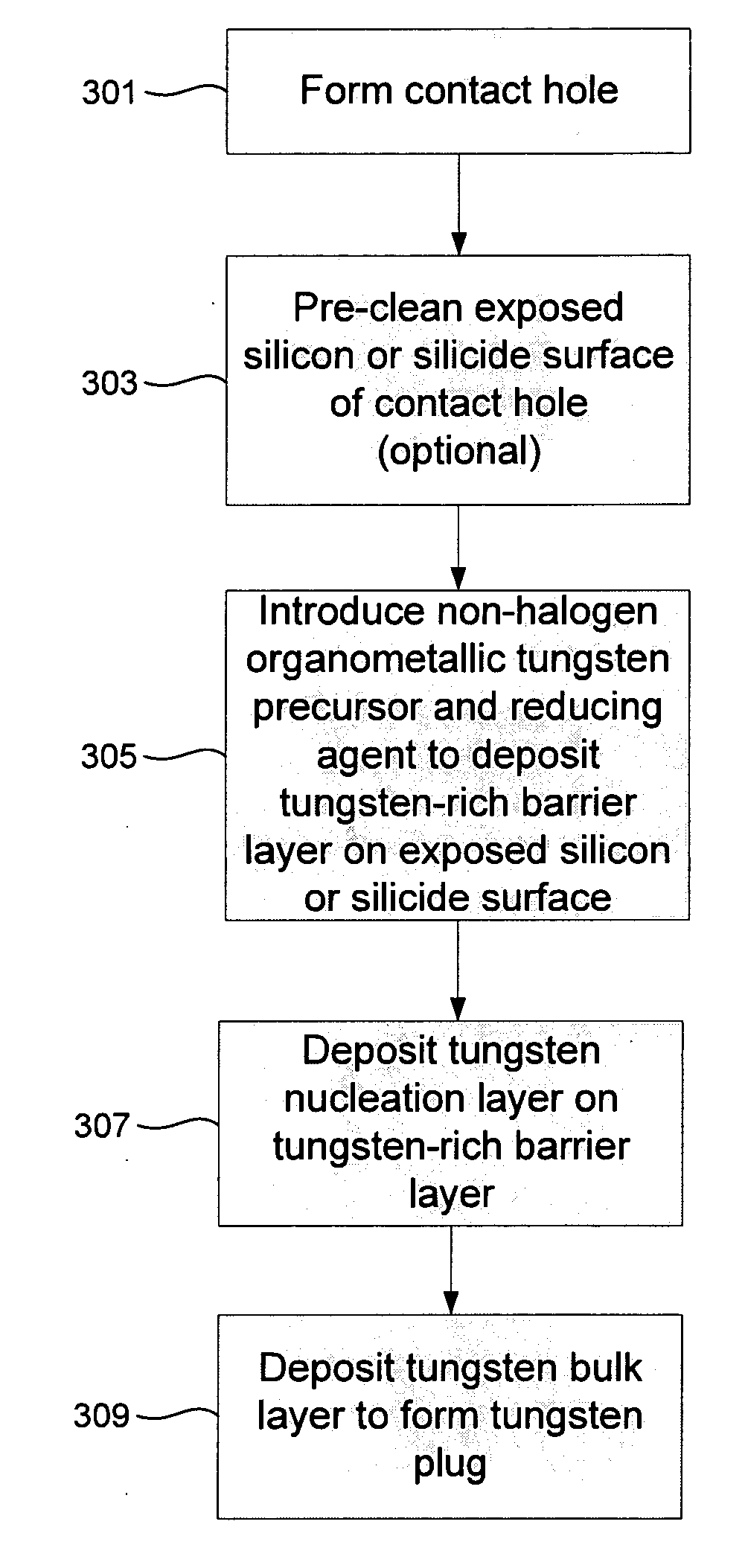
Methods for forming all tungsten contacts and lines
- Summary
- Abstract
- Description
- Claims
- Application Information
AI Technical Summary
Benefits of technology
Problems solved by technology
Method used
Image

Examples
Embodiment Construction
Introduction
[0014]In the following description, numerous specific details are set forth in order to provide a thorough understanding of the invention, which pertains to forming tungsten films. Preferred methods involve exposing a tungsten nucleation layer to pulses of a reducing agent, which will be described in detail below. Modifications, adaptations or variations of specific methods and of structures shown herein will be apparent to those skilled in the art and are within the scope of this invention.
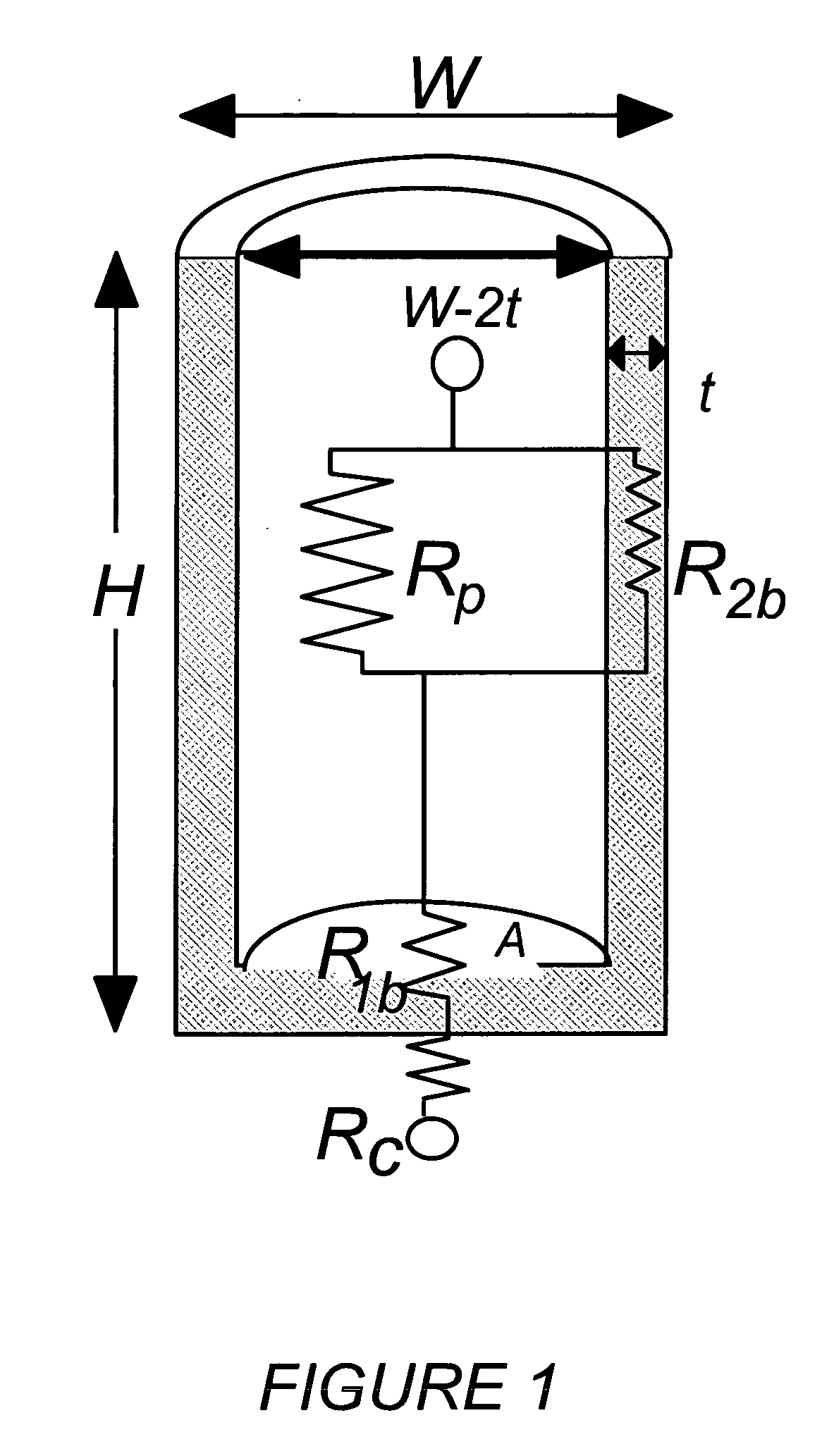
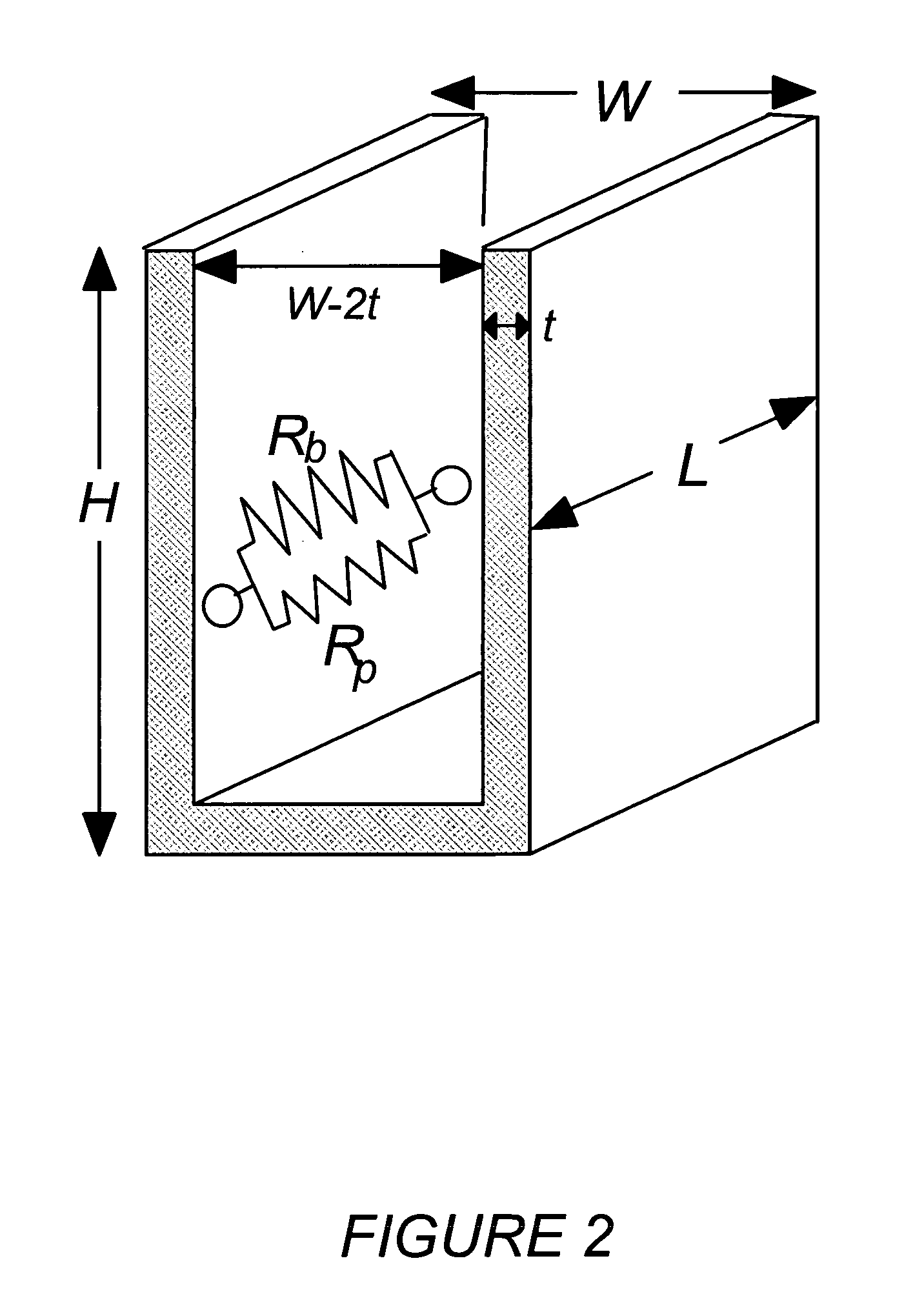
[0015]FIG. 1a is a basic diagram showing contributions to the resistance of a contact via. Rc indicates contact resistance; R1b and R2b the resistance of the barrier layer between the contact and plug; Rp the resistance of the plug; and R3 the resistance of the barrier layer as it extends the length of the plug. Total resistance is given as Rtotal=Rc+R1b+(1 / Rp+1 / R2b)−1. Resistance is equal to ρL / A, where ρ is the resistivity of the material, L is the length of the layer in the directi...
PUM
| Property | Measurement | Unit |
|---|---|---|
| Fraction | aaaaa | aaaaa |
| Percent by atom | aaaaa | aaaaa |
| Percent by atom | aaaaa | aaaaa |
Abstract
Description
Claims
Application Information