

Method of processing semiconductor substrate and processing apparatus
- Summary
- Abstract
- Description
- Claims
- Application Information
AI Technical Summary
Benefits of technology
Problems solved by technology
Method used
Image

Examples
Embodiment Construction
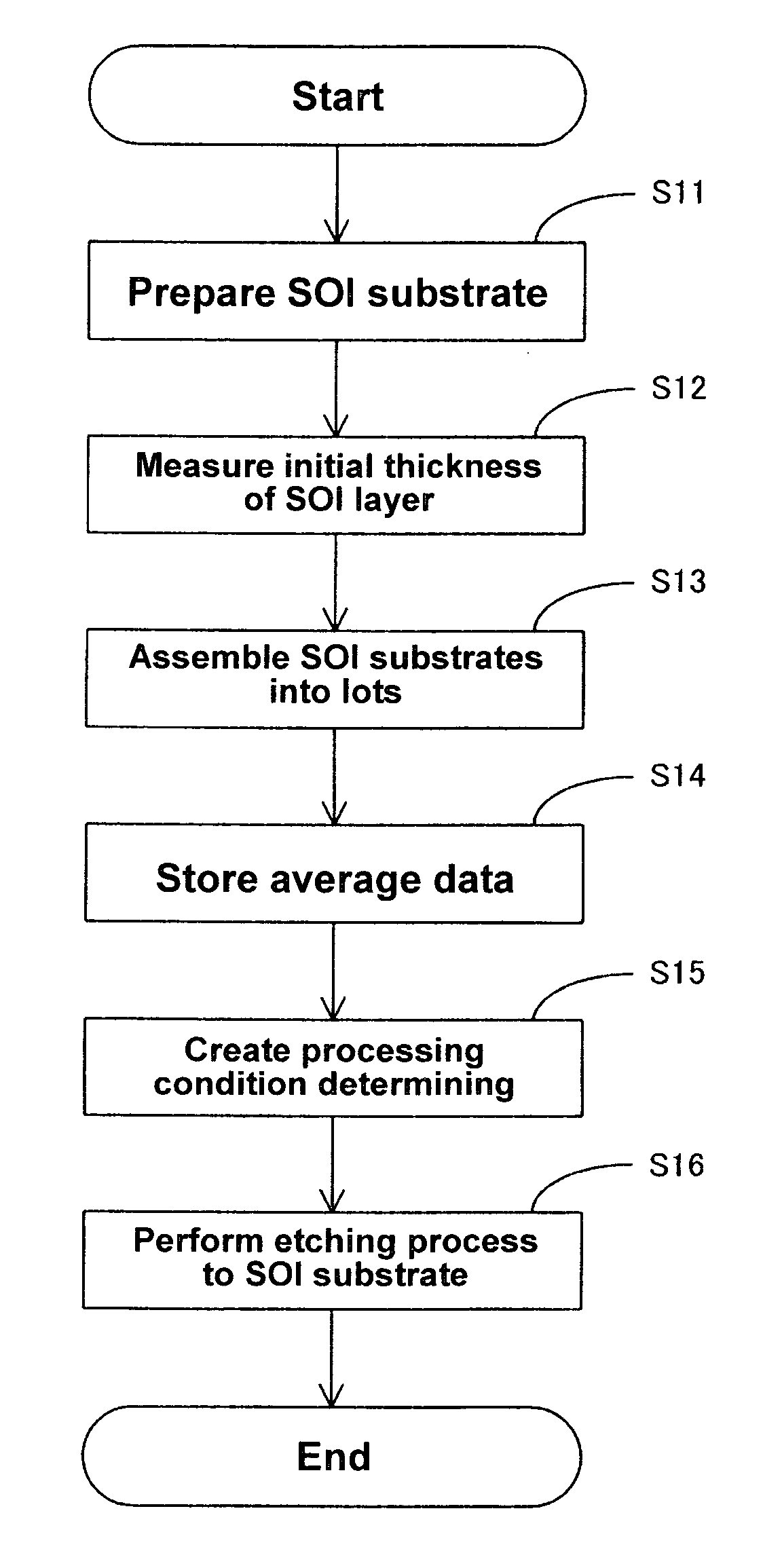
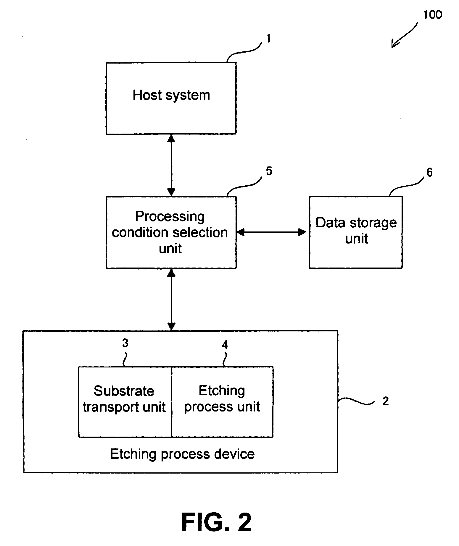
[0033]Hereunder, preferred embodiments of the present invention will be explained with reference to the accompanying drawings. In the following description, substantially similar components or equivalent components are designated with the same reference numerals. FIG. 2 is a block diagram showing a processing apparatus 100 for processing a semiconductor substrate according to an embodiment of the present invention.
[0034]As shown in FIG. 2, the processing apparatus 100 includes a host system 1; an etching process device 2; a processing condition selection unit 5; and a data storage unit 6. The processing condition selection unit 5 is connected for communication to the host system 1, the etching process device 2, and the data storage unit 6. The processing apparatus 100 is configured for processing semiconductor substrates of one single type (one single grade).
[0035]In the embodiment, the host system 1 is a main control unit for controlling the processing apparatus 100 as a whole. The...
PUM
 Abstract
Description
Claims
Application Information