Processing system for fabricating compound nitride semiconductor devices

Inactive Publication Date: 2009-08-06
APPLIED MATERIALS INC
View PDF50 Cites 120 Cited by
  • Summary
  • Abstract
  • Description
  • Claims
  • Application Information

AI Technical Summary

Benefits of technology

[0008]The present invention generally provides an integrated processing system for manufacturing compound nitride semiconductor devices. The processing system comprises one or more walls that form a transfer region that has a robot disposed therein, one or more processing chambers operable to form one or more compound nitride semiconductor layers on a substrate that are in transferable communication with the transfer region, a loadlock chamber in transferable communication with the transfer region, the loadlock chamber having an inlet and an outlet valve to receive at least one substrate into a vacuum environment, and a load station in communication with the loadlock chamber, wherein the load station comprises a conveyor tray movable to convey a carrier plate loaded with one or more substrates into the loadlock chamber.
[0009]Embodiments of the invention further provide an integrated processing system for manufacturing compound nitride semiconductor devices. The processing system comprises one or more walls that form a transfer region that has a robot disposed therein and a first processing chamber that is in communication with the transfer region. The first processing chamber comprises a substrate support positioned within a processing vo

Problems solved by technology

While some modestly successful efforts had previously been made in the production of blue LEDs using SiC materials, such devices suffered from poor luminescence as a consequence of the fact that their electronic structure has an indirect bandgap.
While the feasibility of using GaN to create photoluminescence in the blue region of the spectrum has been known for decades, there were numerous barriers that impeded their practical fabrication.
These barriers included the lack of a suitable substrate on which to grow the GaN structures, generally high thermal requirements for growing GaN that resulted in various

Method used


Image

  • Processing system for fabricating compound nitride semiconductor devices
  • Processing system for fabricating compound nitride semiconductor devices
  • Processing system for fabricating compound nitride semiconductor devices

Examples


Embodiment Construction

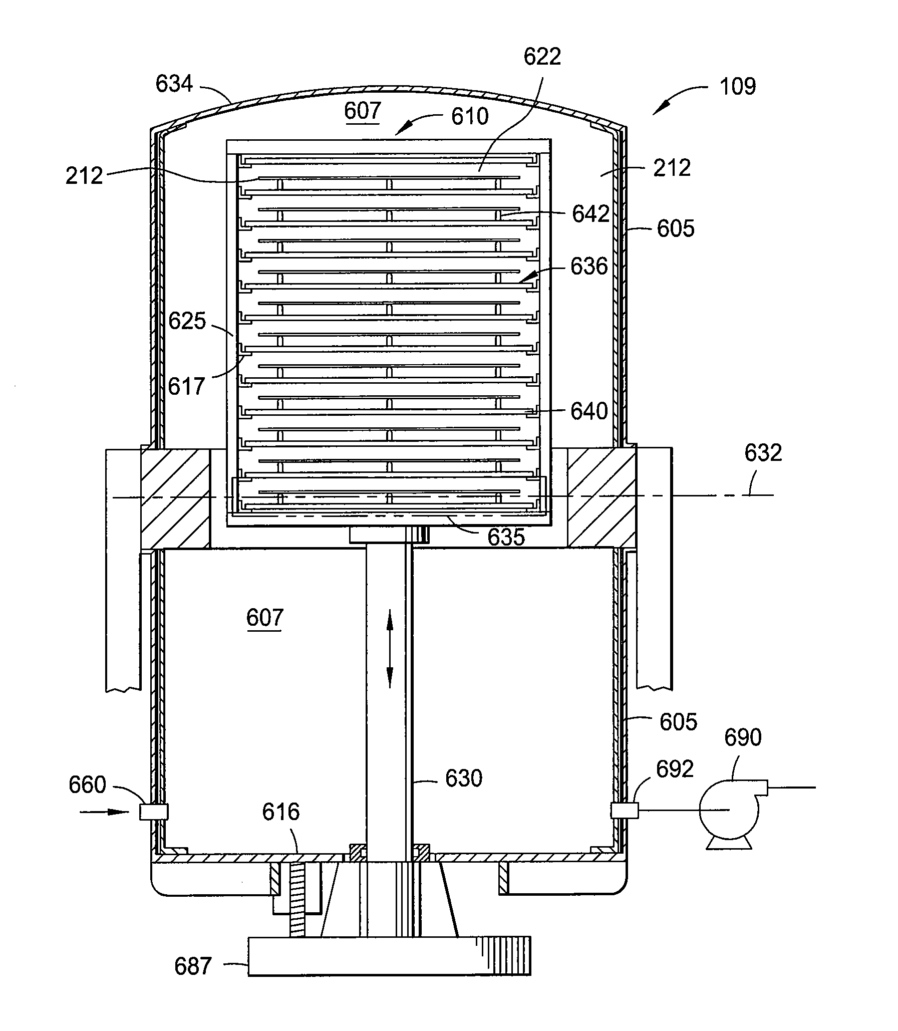
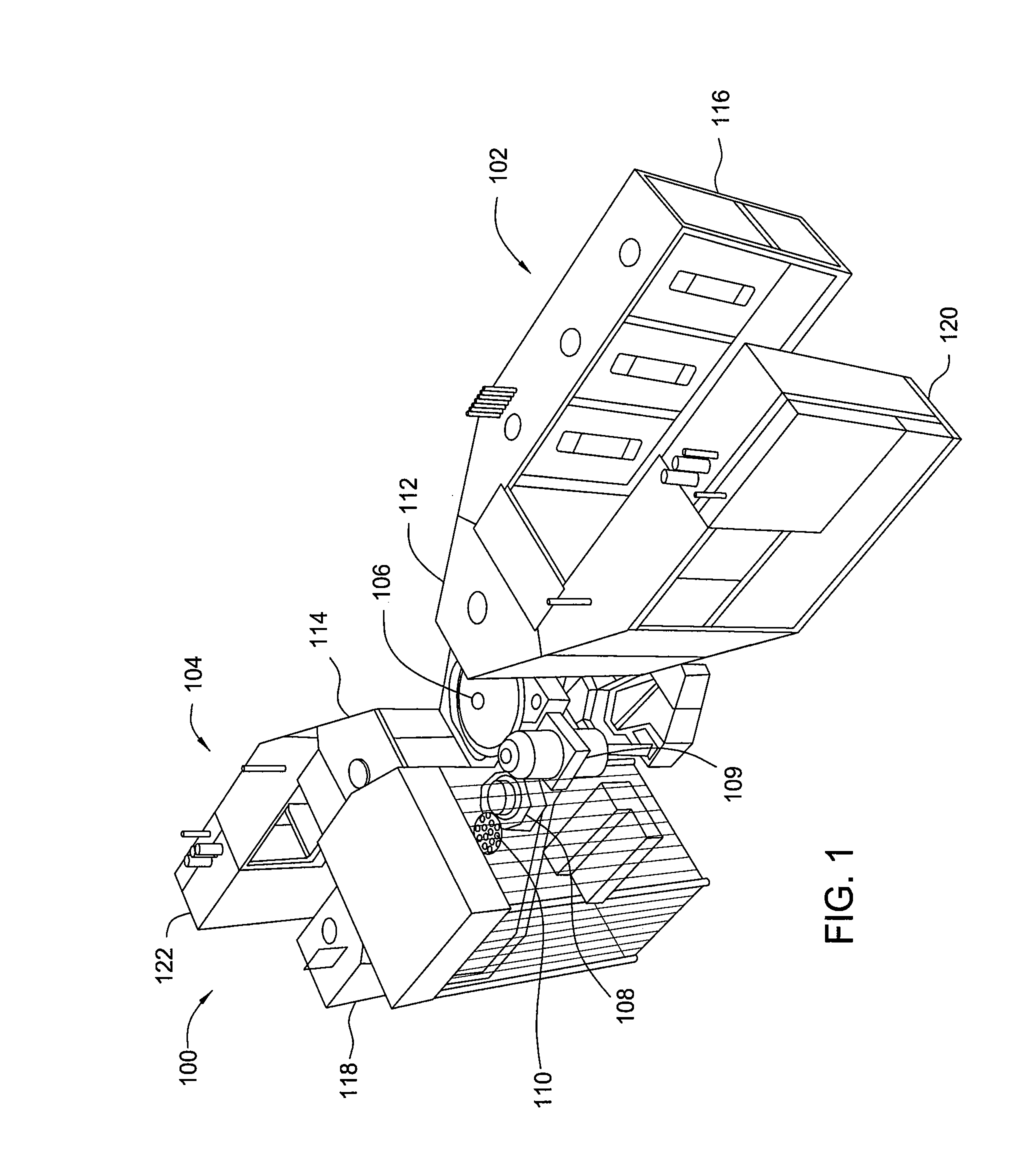
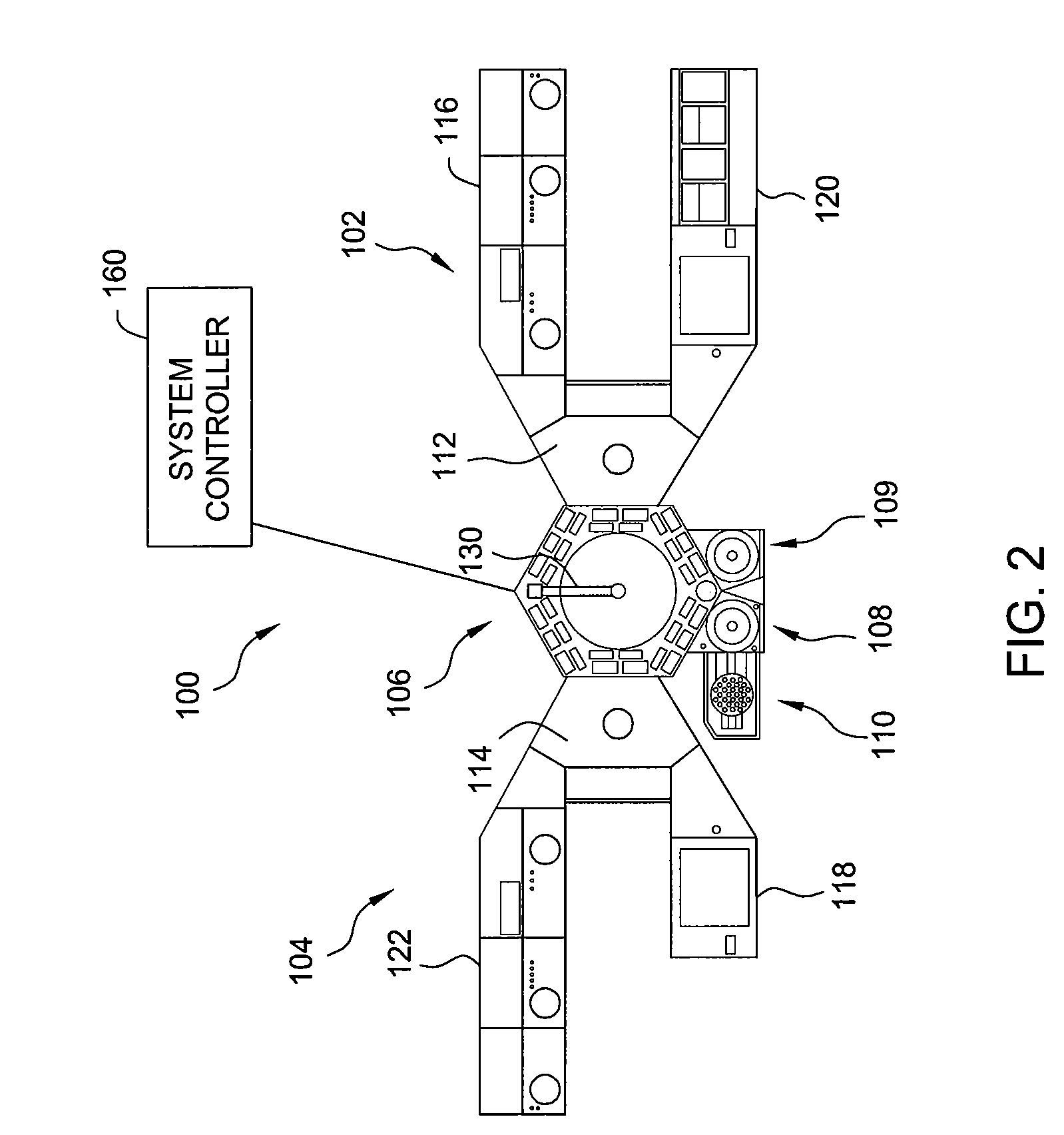
[0025]The present invention generally provides an apparatus and method for simultaneously processing substrates using a multi-chamber processing system (e.g. a cluster tool) that has an increased system throughput, increased system reliability, and increased substrate to substrate uniformity. In one embodiment, the processing system is adapted to fabricate compound nitride semiconductor devices in which a substrate is disposed in a HVPE chamber where a first layer is deposited on the substrate and then the substrate is transferred to a MOCVD chamber where a second layer is deposited over the first layer. In one embodiment, the first layer is deposited over the substrate with a thermal chemical-vapor-deposition process using a first group-III element and a nitrogen precursor and the second layer is deposited over the first layer with a thermal chemical-vapor deposition process using a second group-III precursor and a second nitrogen precursor. Although described in connection to a pr...


PUM

PropertyMeasurementUnit
Forceaaaaaaaaaa
Volumeaaaaaaaaaa
Semiconductor propertiesaaaaaaaaaa

Abstract

One embodiment of a processing system for fabricating compound nitride semiconductor devices comprises one or more processing chamber operable with form a compound nitride semiconductor layer on a substrate, a transfer chamber coupled with the processing chamber, a loadlock chamber coupled with the transfer chamber, and a load station coupled with the loadlock chamber, wherein the load station comprises a conveyor tray movable to convey a carrier plate loaded with one or more substrates into the loadlock chamber. Compared to a single chamber reactor, the multi-chamber processing system expands the potential complexity and variety of compound structures. Additionally, the system can achieve higher quality and yield by specialization of individual chambers for specific epitaxial growth processes. Throughput is increased by simultaneous processing in multiple chambers.

Description

BACKGROUND OF THE INVENTION[0001]1. Field of the Invention[0002]Embodiments of the present invention generally relate to the manufacture of compound nitride semiconductor devices, such as light emitting diodes (LEDs), and, more particularly, to a processing system integrating one or more processing chambers that implement hydride vapor phase epitaxial (HVPE) deposition and / or metal-organic chemical vapor deposition (MOCVD) techniques to fabricate such devices.[0003]2. Description of the Related Art[0004]The history of light-emitting diodes (“LEDs”) is sometimes characterized as a “crawl up the spectrum.” This is because the first commercial LEDs produced light in the infrared portion of the spectrum, followed by the development of red LEDs that used GaAsP on a GaAs substrate. This was, in turn, followed by the use of GaP LEDs with improved efficiency that permitted the production of both brighter red LEDs and orange LEDs. Refinements in the use of GaP then permitted the development ...

Claims


Application Information

Patent Timeline
IPC IPC(8): C23C16/54
CPCC23C16/54C30B25/08H01L21/68771C30B29/403H01L21/68764H01L21/67017H01L21/67115H01L21/67161H01L21/67207C30B35/00
Inventor BURROWS, BRIAN H.WASHINGTON, LORI D.STEVENS, RONALDCHOI, KENRIC T.WHITE, ANTHONY F.ANDERSON, ROGER N.NIJHAWAN, SANDEEPPODESTA, JOSHUA J.TAM, ALEXANDER
Owner APPLIED MATERIALS INC
Why Eureka
Try Eureka