

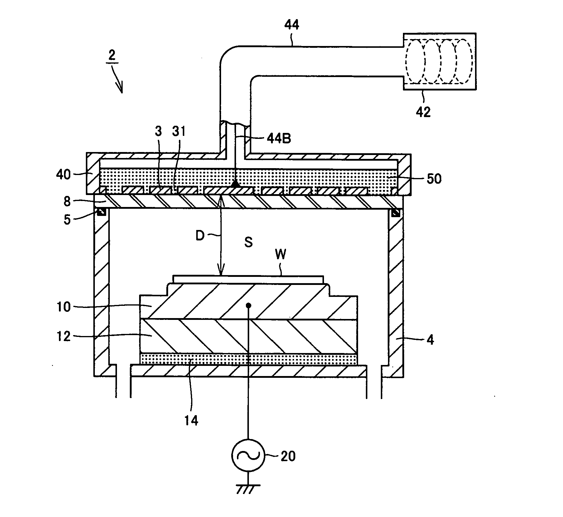
Plasma processing equipment
a processing equipment and plasma technology, applied in plasma technology, energy-based chemical/physical/physico-chemical processes, plasma techniques, etc., can solve the problem that the distribution of plasma in the vicinity of quartz plates b>8/b> cannot be uniformly provided, and achieve the effect of high speed
- Summary
- Abstract
- Description
- Claims
- Application Information
AI Technical Summary
Benefits of technology
Problems solved by technology
Method used
Image

Examples
Embodiment Construction
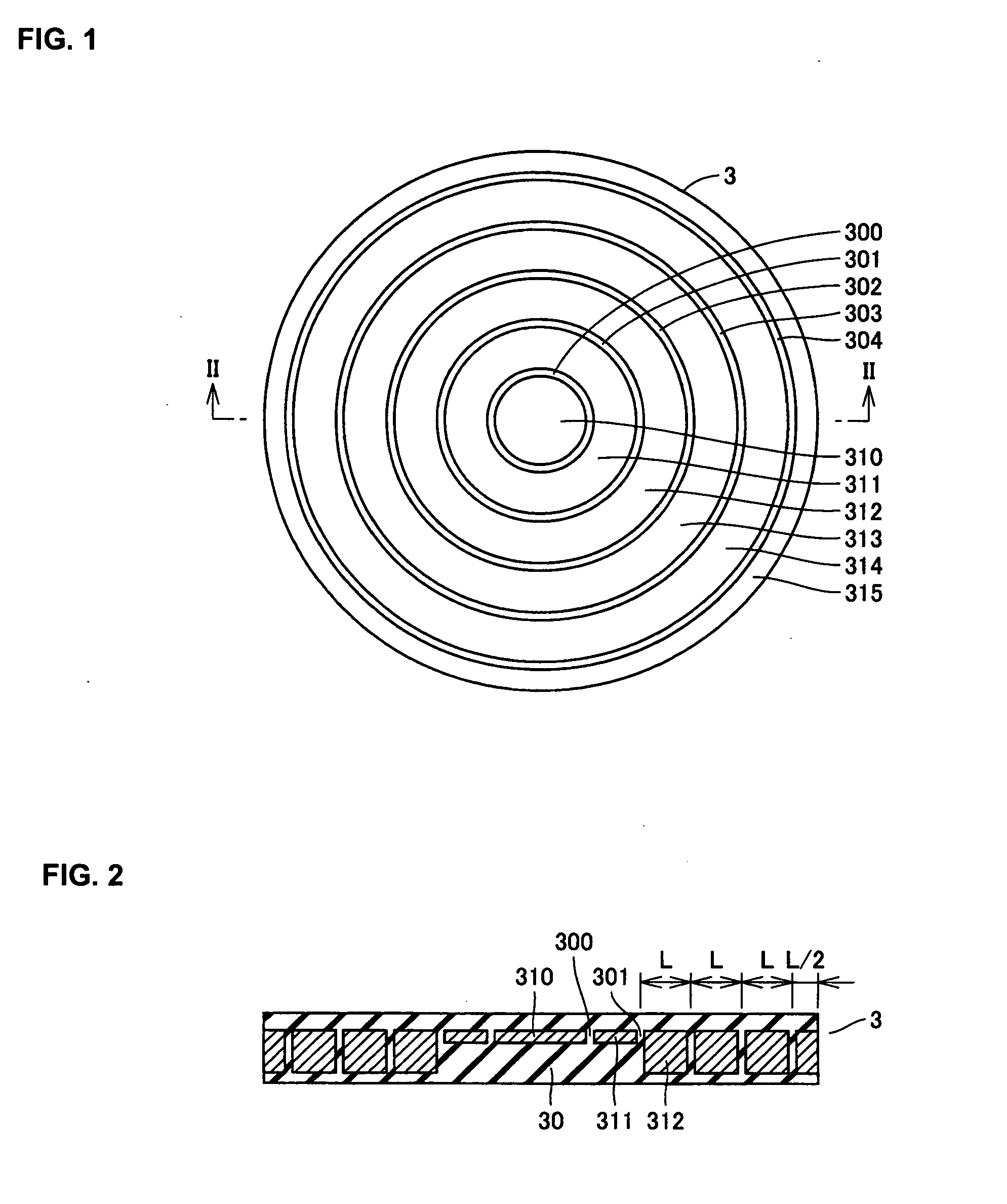
[0044]FIG. 1 is a plan view showing an antenna member used in a plasma processing device according to one embodiment of the present invention, and FIG. 2 is a longitudinal sectional view taken along line II-II in FIG. 1.
[0045]Referring to FIG. 1, an antenna member 3 is formed of an electrically conductive material such as copper, and slots 300 to 304 are formed as a plurality of concentric and closed grooves in the shape of loops to separate the antenna member 3 into an inner conductor region and an outer conductor region. Each of these slots 300 to 304 penetrates the antenna member 3 from one surface to the other surface in the thickness direction and has a width of 1 mm, for example. A distance “L” between the slots 300, 301, 302 and 303 is set to the integral multiple of a guide wavelength of a microwave and more preferably set to the length of the guide wavelength of the microwave, and the distance between the outermost slot 304 and the outer periphery of the antenna member 3 is...
PUM
| Property | Measurement | Unit |
|---|---|---|
| Thickness | aaaaa | aaaaa |
| Electrical conductivity | aaaaa | aaaaa |
| Speed | aaaaa | aaaaa |
Abstract
Description
Claims
Application Information