Structure and Method for Forming Field Effect Transistor with Low Resistance Channel Region

Active Publication Date: 2009-08-06
SEMICON COMPONENTS IND LLC
View PDF31 Cites 29 Cited by
  • Summary
  • Abstract
  • Description
  • Claims
  • Application Information

AI Technical Summary

Benefits of technology

[0018]In accordance with another embodiment of the invention, a method of forming a vertically-conducting planar-gate field effect transistor includes the following steps. A silicon-germanium layer is formed over a silicon region of a first conductivity type. A gate electrode laterally extending over but insulated from the silicon-germanium layer is formed. A body region of a second conductivity type extending in the

Problems solved by technology

Various techniques for reducing the channel resistance and/or the resi

Method used


Image

  • Structure and Method for Forming Field Effect Transistor with Low Resistance Channel Region
  • Structure and Method for Forming Field Effect Transistor with Low Resistance Channel Region
  • Structure and Method for Forming Field Effect Transistor with Low Resistance Channel Region

Examples


Example

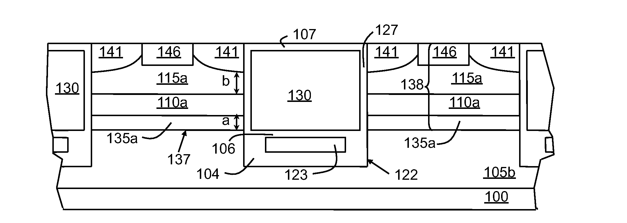
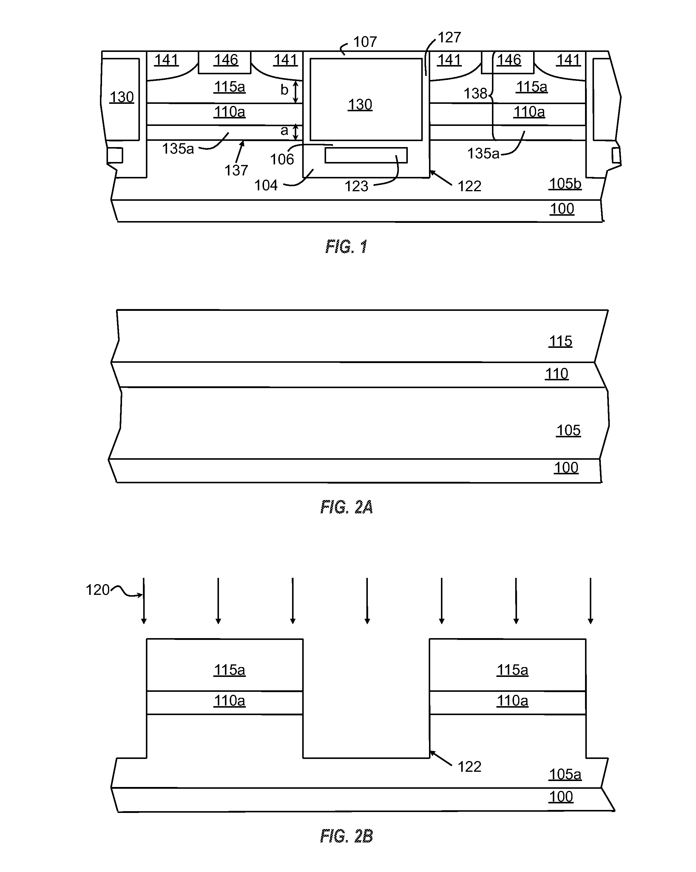
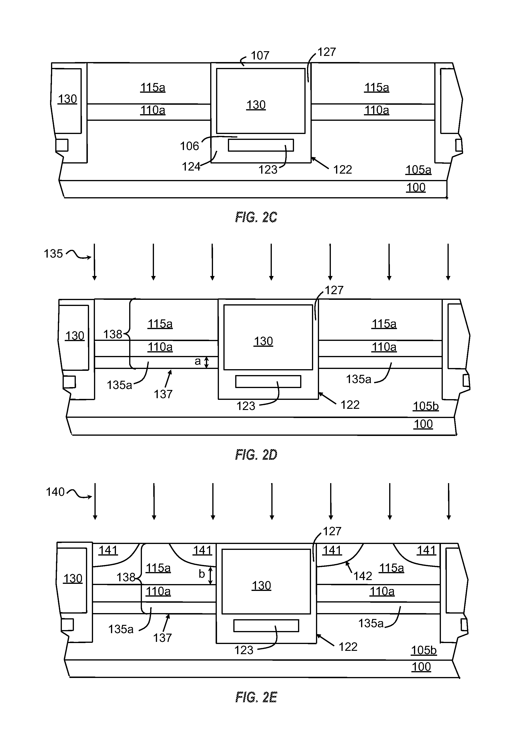
[0028]In accordance with embodiments of the present invention, structures and methods for forming power field effect transistors (such as n-channel and p-channel variations of MOSFETs and IGBTs) with a silicon-germanium layer advantageously integrated therein so as to obtain a low channel resistance are described. In some embodiments, the silicon-germanium layer is embedded in the body region in a particular manner so as to reduce both the channel resistance and the overall resistance of the body region without inducing leakage current or adversely impacting the transistor breakdown voltage. The techniques in accordance with the invention may be implemented in many types of FETs, including both the N-channel and P-channel variations of trench gate, shielded gate and planar gate MOSFETs and IGBTs. Implementation of one exemplary embodiment of the invention in an N-channel shielded gate FET will be described first with reference to FIGS. 1 and 2A-2F.

[0029]FIG. 1 is a simplified cross ...


PUM


Abstract

A trench-gate field effect transistor includes trenches extending into a silicon region of a first conductivity type, and a gate electrodes in each trench. Body regions of second conductivity type extend over the silicon region between adjacent trenches. Each body region forms a first PN junction with the silicon region, and each body region includes a silicon-germanium layer of the second conductivity type laterally extending between adjacent trenches. Source regions of the first conductivity flank the trenches, and each source region forms a second PN junction with one of the body regions. Channel regions extend in the body regions along sidewalls of the trenches between the source regions and a bottom surface of the body regions. The silicon-germanium layers extend into corresponding channel regions to thereby reduce the channel resistance.

Description

CROSS-REFERENCES TO RELATED APPLICATIONS[0001]This application claims the benefit of U.S. Provisional Application No. 61 / 013,411, filed Dec. 13, 2007, which is incorporated herein by reference in its entirety for all purposes.BACKGROUND OF THE INVENTION[0002]The present invention relates in general to semiconductor structures and methods for forming the same, and more particularly to semiconductor power field effect transistors (FETs) with low resistance channel regions.[0003]Some conventional vertically conducting trench-gate power MOSFETs include an n-type substrate over which an n-type epitaxial layer extends. The substrate embodies the drain of MOSFET. A p-type body region extends into the epitaxial layer. Trenches extend through the body region and into the portion of the epitaxial layer bounded by the body region and the substrate (commonly referred to as the drift region). A dielectric layer lines the sidewalls and bottom of each trench. Gate electrodes (e.g., from polysilico...

Claims


Application Information

Patent Timeline
IPC IPC(8): H01L29/78
CPCH01L21/26506H01L29/165H01L29/407H01L29/42368H01L29/7813H01L29/66719H01L29/66734H01L29/7397H01L29/7802H01L29/66712H01L21/2652
Inventor PAN, JAMESWANG, QI
Owner SEMICON COMPONENTS IND LLC
Why Eureka
Try Eureka