Optical integrated nanospectrometer and method of manufacturing thereof

a nano-spectrometer and optical chip technology, applied in the field of optical spectrometry, can solve the problems of increasing intrinsic losses, unable to extend this type of optical chip to a large number of channels, and unable to achieve the effect of suppressing crosstalk

Inactive Publication Date: 2009-08-06
OOO NANOOPTIC DEVICES
View PDF7 Cites 25 Cited by
  • Summary
  • Abstract
  • Description
  • Claims
  • Application Information

AI Technical Summary

Benefits of technology

[0022]The present invention further provides the step of correcting crosstalk by imposing a linear relationship on geometrical positions of input / output ports and central frequencies of channels. According to another modification of the present invention, crosstalk can be suppressed by precompensation of generating function A(x,y).
[0023]With use of the above-described super-grating, the present invention makes it possible to develop nanospectrometers of different types that can be integrated on a chip for detection of solid, liquid, or gas analytes. Examples of these nanospectrometers are the following: a laser-induced breakdown (LIB) spectrometer, an absorption spectrometer, or a Raman spectrometer.

Problems solved by technology

In principle, this type of optical chip can be used as a spectral device for limited amount of wavelengths; however, extending this type of optical chip to a large number of channels is not feasible, and this is the main disadvantage of the approach.
As the number of channels and correspondingly the number of wavelengths to be processed grows, the size of the device increases, the path of light to the remote gratings grows, and, consequently, intrinsic losses grow as well.
Also, building large devices is difficult and expensive due to limited precision of the lithographic process and limited uniformity of the waveguide used for gratings.
The remaining two patents do not teach a compact spectrometer.
A common disadvantage of the above-described known optical spectrometers is their relatively large dimensions, and the applicants are unaware of the existence of miniature optical planar spectrometers designed and operating on the principle of digital planar holography.

Method used


Image

  • Optical integrated nanospectrometer and method of manufacturing thereof
  • Optical integrated nanospectrometer and method of manufacturing thereof
  • Optical integrated nanospectrometer and method of manufacturing thereof

Examples


Embodiment Construction

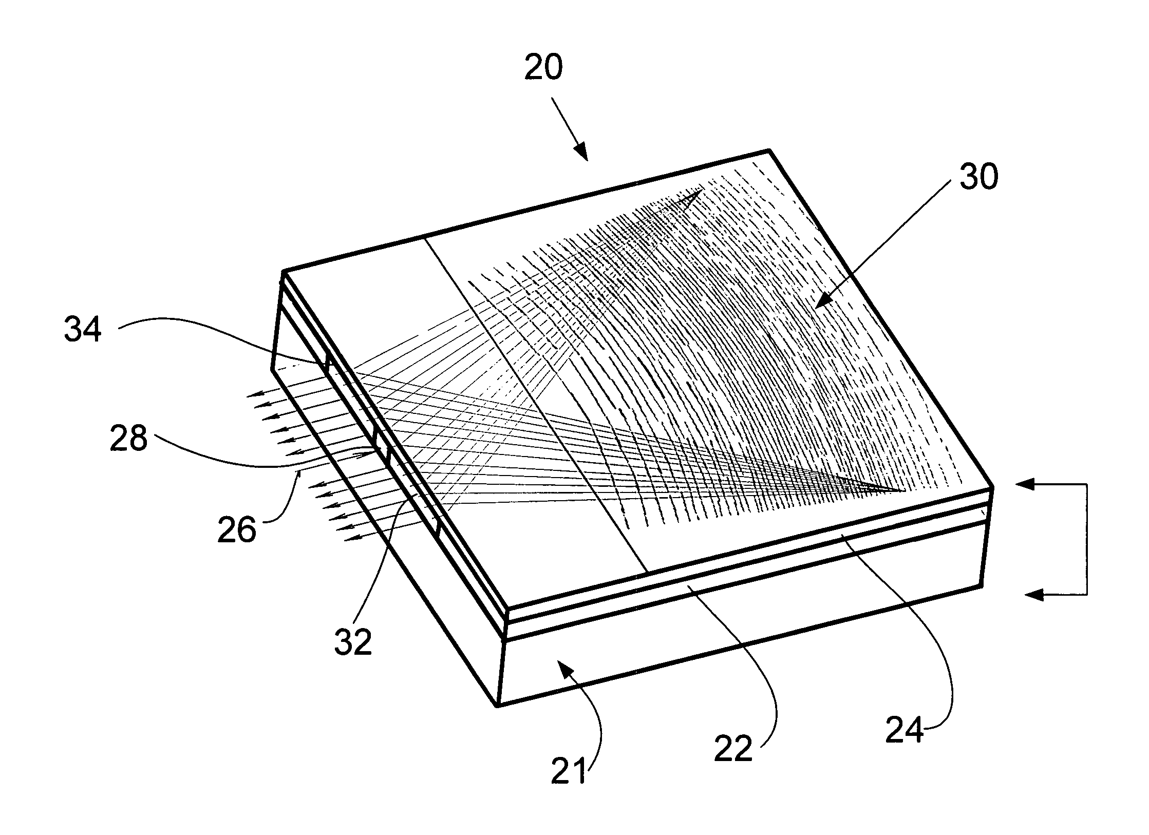
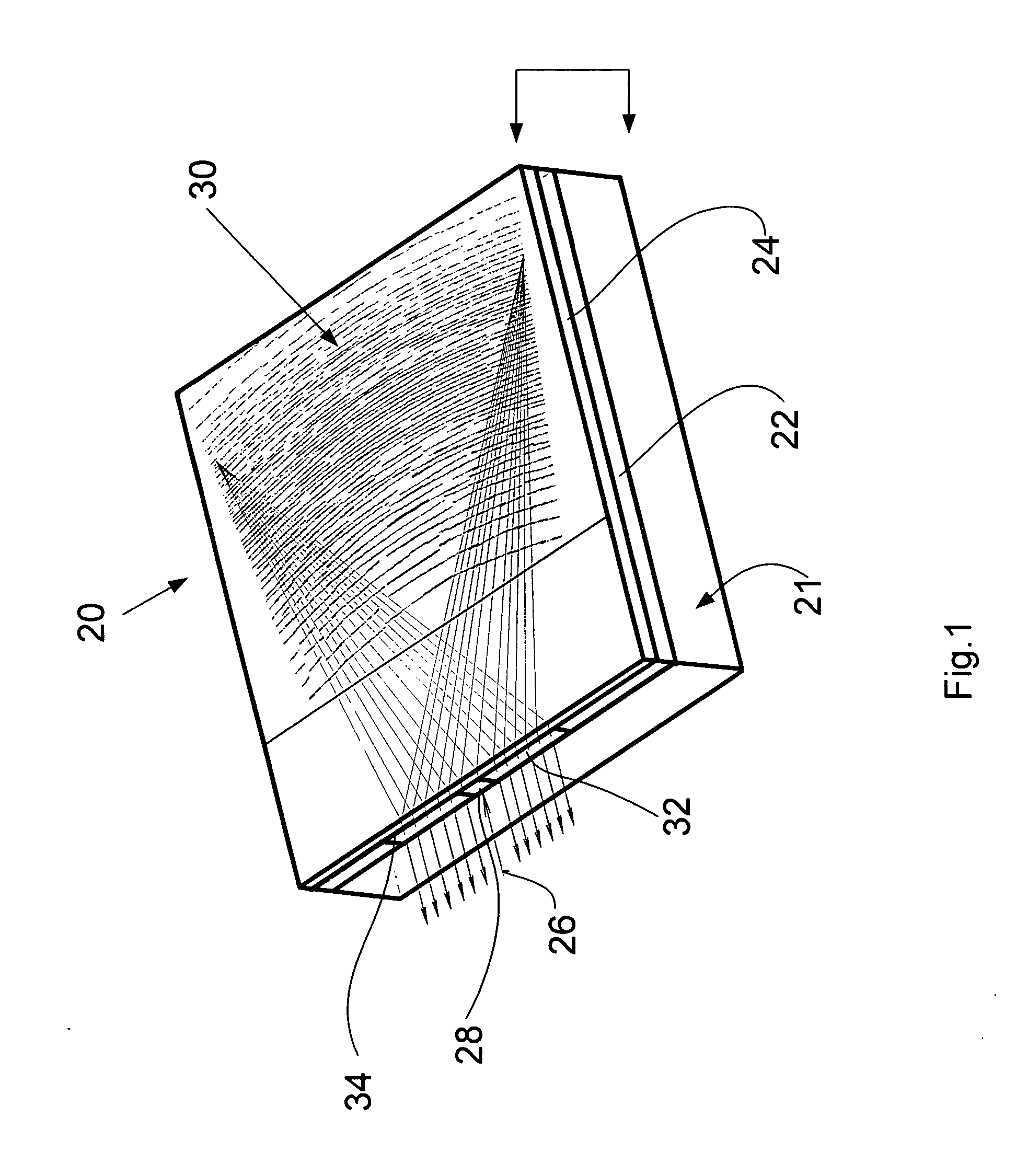
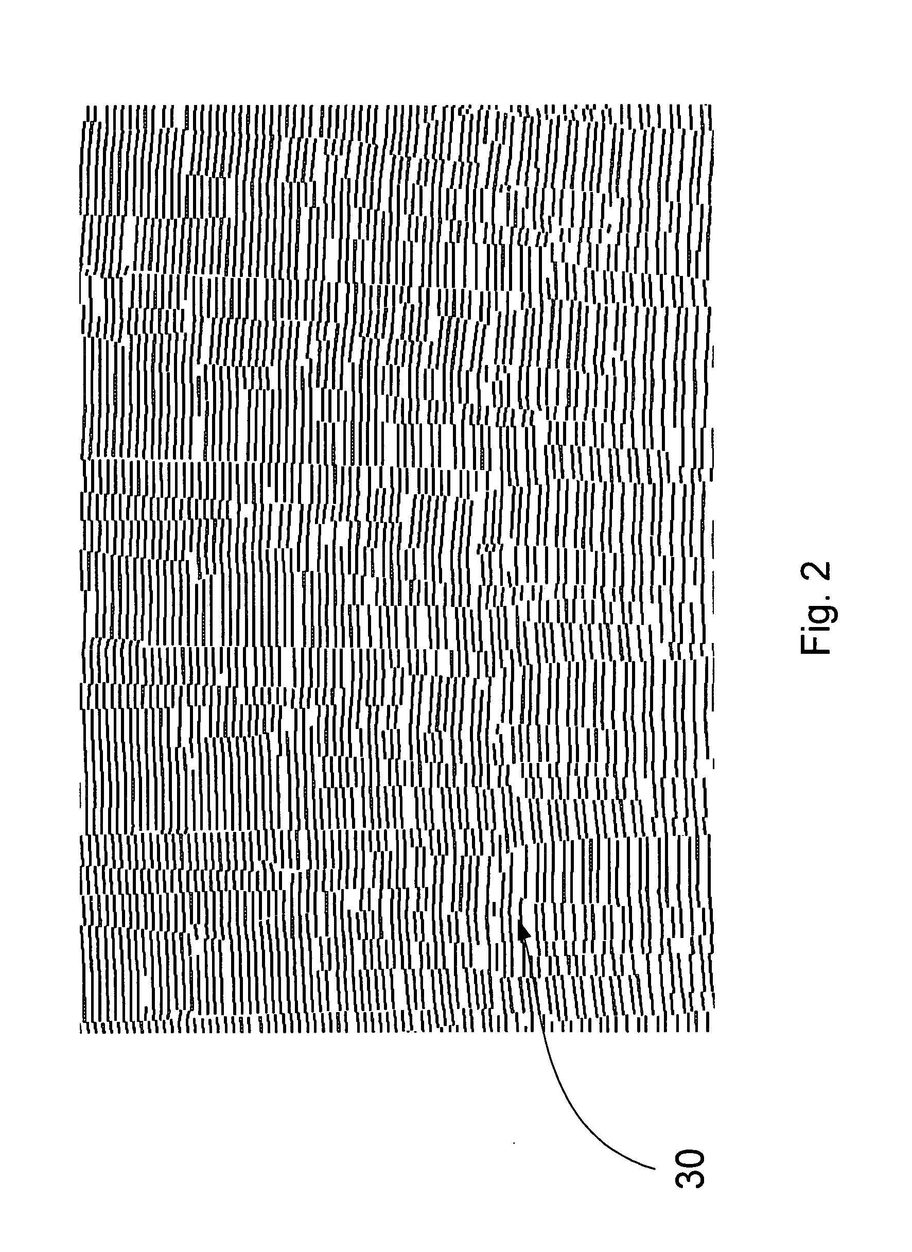
[0039]In the context of the present invention, the term “super-grating” means a digital planar hologram that performs multiple functions and operates for a plurality of channels incorporated into a nanospectrometer.

[0040]In the context of the present invention, the term “sub-grating” means a virtual component of the aforementioned digital planar hologram that provides operation of a single light-signal-transmitting channel. The same elements of different sub-gratings belong to the same super-grating.

[0041]The physics of a spectral super-grating, deployed in the invented spectrometers, is complicated, and for this reason several theoretical models should be used to explain the properties of transfer function. In a first approximation, the super-grating works like a superposition of elliptical sub-gratings, each of which connects an input port with one of multiple output ports. The sub-gratings are structures that are composed of multiple nano-features that modulate the refractive ind...


PUM

PropertyMeasurementUnit
volumeaaaaaaaaaa
wavelengthaaaaaaaaaa
depthaaaaaaaaaa

Abstract

A planar nanospectrometer formed as a single chip that uses diffraction structures, which are combinations of numerous nano-features placed in a predetermined configuration and providing multiple functionalities such as guiding light, resonantly reflecting light at multiple wavelengths, directing light to detectors, and focusing light on the detectors. The diffraction structure can be described as a digital planar hologram that comprises an optimized combination of overlaid virtual sub-gratings, each of which is resonant to a single wavelength of light. Each device includes at least one sensor, at least one light source, and at least one digital planar hologram in an optical waveguide. The device of the present invention allows detection of small amounts of analytes in gases and liquids or on solid surfaces and can be particularly advantageous for field analysis of environmental safety in multiple locations because of its miniature size and low cost.

Description

CROSS REFERENCE TO RELATED APPLICATIONS[0001]The present patent application is related to the following pending patent applications: (1) U.S. patent application Ser. No. 405,160 filed by V. Yankov et al on Apr. 2, 2003 entitled “Planar holographic multiplexer / demultiplexer”; (2) U.S. patent application Ser. No. 137,152 filed by S. Babin et al on May 2, 2002 entitled: “Photonic multi-bandgap lightwave device and methods for manufacturing thereof”; and (3) U.S. patent application Ser. No. 167,773 filed by L. Polonskiy et al on Jun. 11, 2002 entitled: “Integrating elements for optical fiber communication.”FIELD OF THE INVENTION[0002]The present invention generally relates to optical spectrometry for detecting small quantities of analytes and for other related applications. In particular, the present invention provides a miniature integrated optical spectrometer based on nano-structures embedded into planar waveguides.BACKGROUND INFORMATION[0003]Last century witnessed multiple improveme...

Claims


Application Information

Patent Timeline
Patent Type & Authority Applications(United States)
IPC IPC(8): G01J3/28G02B6/12G01J3/44B29D11/00
CPCG01N21/253G01N21/31G01N21/552G01N21/65G01N21/658G02B6/124G01N21/774G01N2201/0221G01N2201/088G02B6/12007G01N21/7703
Inventor YANKOV, VLADIMIR
Owner OOO NANOOPTIC DEVICES
Why Eureka
Try Eureka