Semiconductor device

a technology of semiconductor devices and semiconductors, applied in the direction of instruments, heat measurement, thermometer details, etc., can solve the problems of large time and cost that is required for tuning, and complicated control thereof, so as to reduce detection temperature, prevent cost increase, and increase the size of tuning circuits

Inactive Publication Date: 2009-08-06
RENESAS ELECTRONICS CORP
View PDF10 Cites 28 Cited by
  • Summary
  • Abstract
  • Description
  • Claims
  • Application Information

AI Technical Summary

Benefits of technology

[0009]By adding a raising circuit to the tuning circuit, it is possible to raise the voltage of a third signal by a certain level and greatly decrease a detection temperature in a test mode without changing the circuit size of the tuning circuit. Even in the case where the detection temperature changes greatly between the test mode and the normal mode, without increasing the size of the tuning circuit it is possible to prevent a cost increase, maintain a high tuning accuracy, and suppress an increase in the time required for tuning.

Problems solved by technology

However, to extend the tuning range or enhance the tuning accuracy, the tuning circuit becomes larger in size or the control thereof becomes complicated, which disadvantageously requires time and cost for tuning.

Method used


Image

  • Semiconductor device
  • Semiconductor device
  • Semiconductor device

Examples


first embodiment

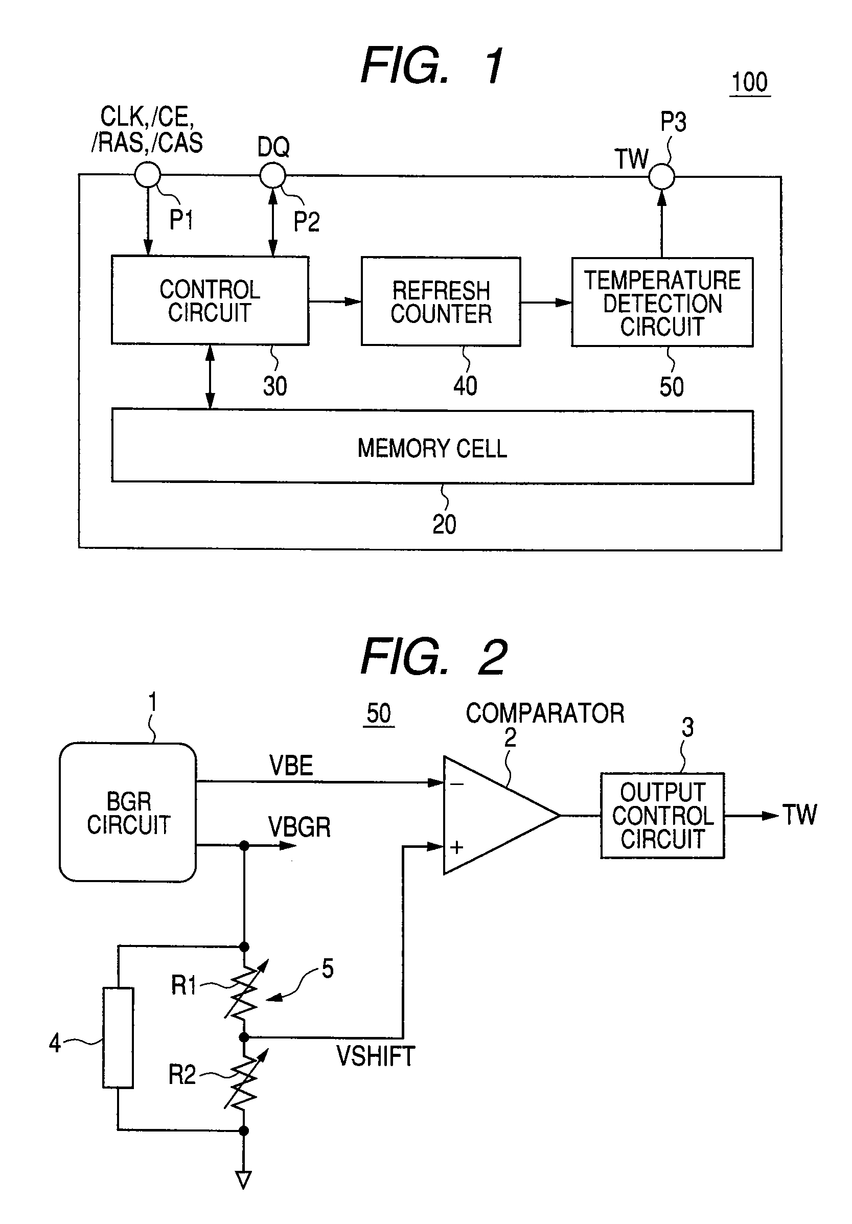
[0065]Next, the configuration and operation of a temperature detection circuit according to the first embodiment of the invention will be described with reference to FIGS. 8 to 12.

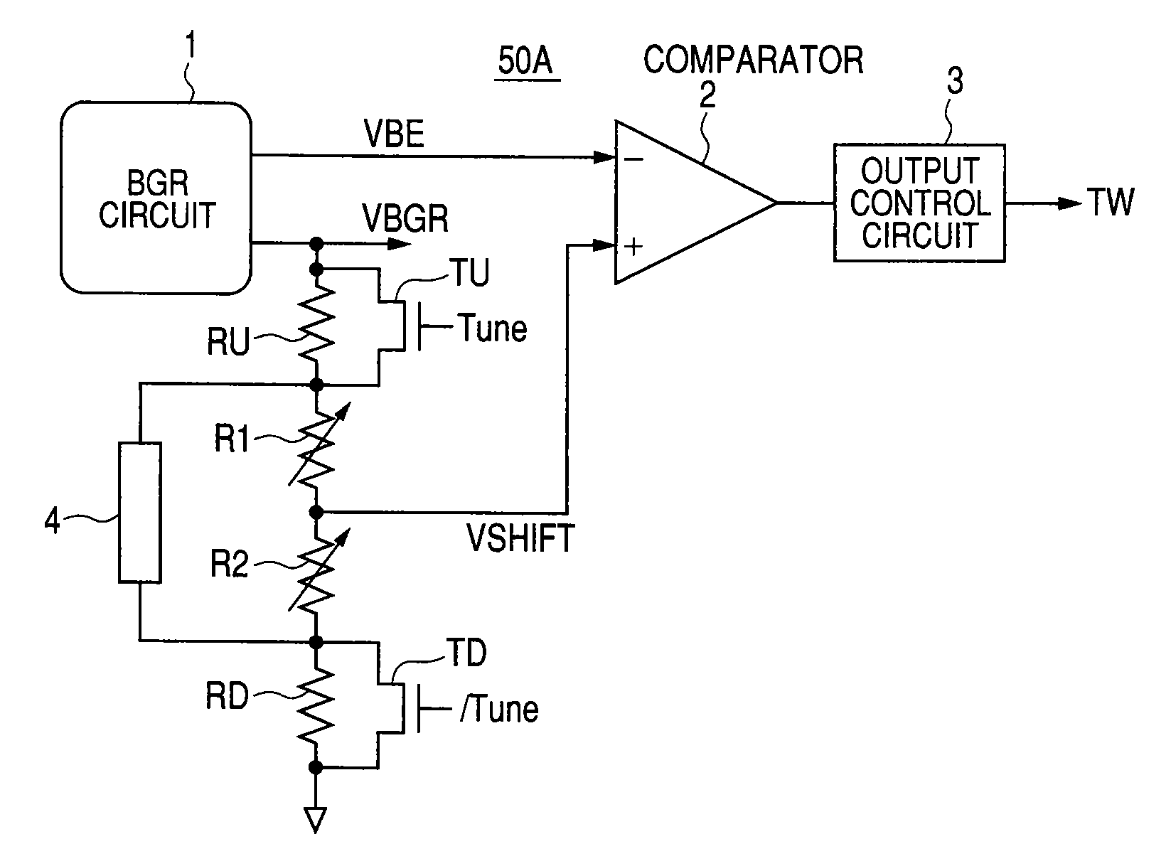
[0066]FIG. 8 is a block diagram showing the configuration of a temperature detection circuit 50A according to the first embodiment. The same configurations as in the temperature detection circuit 50 described with reference to FIG. 2 are denoted by the same reference numerals, and their description will not be repeated.

[0067]Further, the temperature detection circuit 50A can be substituted for the temperature detection circuit 50 of the memory chip 100 shown in FIG. 1. The temperature detection circuit 50A shown in FIG. 8 has, in addition to the variable resistors R1 and R2 configuring the level shift circuit 5, an additional resistor RU (a first resistor) coupled between the output node of the VBGR voltage of the BGR circuit 1 and the variable resistor R1 and an additional resistor RD (a second resistor) ...

second embodiment

[0088]Next, the configuration and operation of a temperature detection circuit according to the second embodiment of the invention will be described with reference to FIGS. 13 to 16.

[0089]FIG. 13 is a block diagram showing the configuration of a temperature detection circuit 50B according to the second embodiment. The same configurations as in the temperature detection circuit 50A described with reference to FIG. 8 are denoted by the same reference numerals, and their description will not be repeated.

[0090]In the temperature detection circuit 50B shown in FIG. 13, a comparator 2A has a hysteresis characteristic in the normal mode and does not have a hysteresis characteristic in the test mode.

[0091]FIG. 14 shows that the VSHIFT voltage is increased in the test mode so that the point of intersection of the VSHIFT voltage and the VBE voltage, that is, the detection temperature changes to 85° C. In FIG. 14, the horizontal axis indicates the temperature (° C.), and the vertical axis indi...

third embodiment

[0098]Next, the configuration and operation of a temperature detection circuit according to the third embodiment of the invention will be described with reference to FIGS. 17 to 21.

[0099]FIG. 17 is a block diagram showing the configuration of a temperature detection circuit 50C according to the third embodiment. The same configurations as in the temperature detection circuit 50A described with reference to FIG. 8 are denoted by the same reference numerals, and their description will not be repeated.

[0100]In the temperature detection circuit 50 shown in FIG. 2 and the temperature detection circuit 50A shown in FIG. 8, the determination result of the chip inside temperature is not outputted in real time in the normal mode, but the output control circuit 3 updates the determination result at predetermined intervals in synchronization with rising edges of an upper counter of the refresh counter 40 in the memory chip 100 (FIG. 1) and outputs it to the outside.

[0101]On the other hand, an ...


PUM

PropertyMeasurementUnit
temperatureaaaaaaaaaa
voltageaaaaaaaaaa
resistance valueaaaaaaaaaa

Abstract

There is provided a semiconductor device which can maintain a high tuning accuracy while suppressing a cost increase and suppress an increase in the time required for tuning. There are included, in addition to variable resistors configuring a level shift circuit, an additional resistor coupled between the output node of a VBGR voltage of a BGR circuit and one of the variable resistors and an additional resistor coupled between the other of the variable resistors and a reference voltage. N-channel MOS transistors are coupled in parallel with the additional resistors, respectively.

Description

CROSS-REFERENCE TO RELATED APPLICATIONS [0001]The disclosure of Japanese Patent Application No. 2008-23750 filed on Feb. 4, 2008 including the specification, drawings and abstract is incorporated herein by reference in its entirety.BACKGROUND OF THE INVENTION[0002]The present invention relates to a semiconductor device, and in particular, relates to a semiconductor device having a temperature detection circuit which, when the temperature of a semiconductor chip exceeds a predetermined temperature, informs the outside accordingly.[0003]In recent years, in a memory chip for SiP (system in package) incorporating a microprocessor and sensors as well as memory in one package, the function of outputting the information when the chip inside temperature exceeds a predetermined temperature to a control apparatus (microprocessor or the like) for controlling the memory has been required.[0004]As an example of a temperature detection circuit, FIGS. 1 to 4 in Japanese Unexamined Patent Publicati...

Claims


Application Information

Patent Timeline
Patent Type & Authority Applications(United States)
IPC IPC(8): G01K7/00
CPCG01K7/015G01K3/005
Inventor TSUKUDE, MASAKI
Owner RENESAS ELECTRONICS CORP
Why Eureka
Try Eureka